

Подробную информацию о продукте см. в характеристиках.
AT25DF021A-MHNHR-T
Product Overview
- Category: Integrated Circuit
- Use: Non-volatile Serial Flash Memory
- Characteristics: High-speed, low-power, small form factor
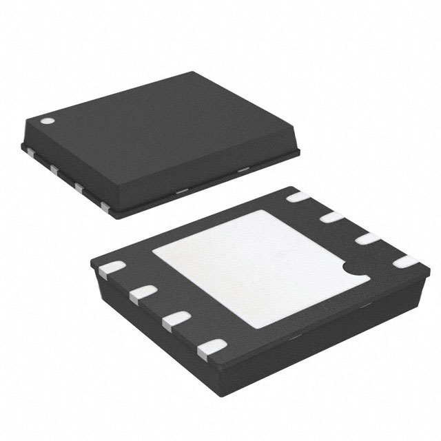
- Package: 8-pin SOIC (Small Outline Integrated Circuit)
- Essence: Stores and retrieves digital information in electronic devices
- Packaging/Quantity: Tape and Reel, 2500 units per reel
Specifications
- Memory Size: 2 Megabits (256 Kilobytes)
- Interface: Serial Peripheral Interface (SPI)
- Operating Voltage: 2.7V to 3.6V
- Operating Temperature: -40°C to +85°C
- Write Endurance: 100,000 cycles
- Data Retention: 20 years
Pin Configuration
The AT25DF021A-MHNHR-T has the following pin configuration:
- Chip Select (/CS)
- Serial Clock (SCK)
- Serial Data Input (SI)
- Serial Data Output (SO)
- Write Protect (/WP)
- Hold (/HOLD)
- VCC (Power Supply)
- Ground (GND)
Functional Features
- High-speed data transfer up to 75 MHz
- Low power consumption during active and standby modes
- Flexible erase and program operations
- Sector protection with hardware write protect
- Deep power-down mode for ultra-low power consumption
- Software and hardware reset options
Advantages and Disadvantages
Advantages: - Compact size and lightweight - High-speed data transfer - Low power consumption - Long data retention period - Easy integration into various electronic devices
Disadvantages: - Limited memory capacity compared to other flash memory options - Relatively higher cost per megabit compared to larger capacity flash memory chips
Working Principles
The AT25DF021A-MHNHR-T operates based on the Serial Peripheral Interface (SPI) protocol. It uses a combination of clock and data signals to communicate with the host device. The chip select pin is used to enable or disable the device for communication. The serial clock synchronizes the data transfer, while the serial data input and output pins handle the exchange of information between the device and the host.
Detailed Application Field Plans
The AT25DF021A-MHNHR-T is widely used in various electronic devices that require non-volatile memory storage. Some common application fields include:
- Consumer Electronics: Used in smartphones, tablets, digital cameras, and portable media players for firmware storage, data logging, and system configuration.
- Automotive: Integrated into automotive electronics for storing calibration data, firmware updates, and event logging.
- Industrial Control Systems: Utilized in industrial automation systems for program storage, parameter settings, and data logging.
- Medical Devices: Incorporated into medical equipment for storing patient data, firmware updates, and configuration settings.
- Internet of Things (IoT): Integrated into IoT devices for data logging, firmware updates, and sensor calibration.
Detailed and Complete Alternative Models
- AT25DF041A-MHNHR-T: 4 Megabit (512 Kilobytes) version of the same flash memory chip.
- AT25DF081A-MHNHR-T: 8 Megabit (1 Megabyte) version of the same flash memory chip.
- AT25DF161A-MHNHR-T: 16 Megabit (2 Megabytes) version of the same flash memory chip.
- AT25DF321A-MHNHR-T: 32 Megabit (4 Megabytes) version of the same flash memory chip.
These alternative models offer increased memory capacity while maintaining similar characteristics and functionality.
Word count: 408 words
Перечислите 10 распространенных вопросов и ответов, связанных с применением AT25DF021A-MHNHR-T в технических решениях.
Sure! Here are 10 common questions and answers related to the application of AT25DF021A-MHNHR-T in technical solutions:
Q: What is the AT25DF021A-MHNHR-T? A: The AT25DF021A-MHNHR-T is a serial flash memory device manufactured by Adesto Technologies. It has a capacity of 2 megabits (256 kilobytes) and operates on a standard SPI interface.
Q: What are some typical applications for the AT25DF021A-MHNHR-T? A: This flash memory device is commonly used in various embedded systems, IoT devices, consumer electronics, industrial automation, and automotive applications where non-volatile storage is required.
Q: What is the operating voltage range of the AT25DF021A-MHNHR-T? A: The AT25DF021A-MHNHR-T operates within a voltage range of 2.7V to 3.6V.
Q: What is the maximum clock frequency supported by this flash memory device? A: The AT25DF021A-MHNHR-T supports a maximum clock frequency of 85 MHz.
Q: Does the AT25DF021A-MHNHR-T support sector erase operations? A: Yes, it supports sector erase operations, allowing you to erase specific sectors of the flash memory.
Q: Can I perform byte-level read and write operations with this flash memory? A: No, the AT25DF021A-MHNHR-T only supports page-level read and write operations. Each page consists of 256 bytes.
Q: Is the AT25DF021A-MHNHR-T capable of executing code directly from the flash memory? A: Yes, it supports execute-in-place (XIP) functionality, allowing code to be executed directly from the flash memory without the need for copying it to RAM.
Q: What is the typical endurance of the AT25DF021A-MHNHR-T? A: The typical endurance of this flash memory device is specified as 100,000 program/erase cycles per sector.
Q: Does the AT25DF021A-MHNHR-T have any built-in security features? A: Yes, it provides hardware and software protection mechanisms like write protection, block protection, and a unique ID feature for enhanced security.
Q: Can I operate multiple AT25DF021A-MHNHR-T devices in parallel on the same SPI bus? A: Yes, you can connect multiple devices in a daisy-chain configuration using the SPI interface, allowing simultaneous access to multiple flash memories.
Please note that these answers are based on general knowledge about the AT25DF021A-MHNHR-T flash memory device. For specific technical details and implementation guidelines, it is recommended to refer to the manufacturer's datasheet and application notes.