

Подробную информацию о продукте см. в характеристиках.
AD9683BCPZRL7-250
Product Overview
Category
AD9683BCPZRL7-250 belongs to the category of integrated circuits (ICs).
Use
This product is primarily used in high-speed analog-to-digital converters (ADCs) for various applications.
Characteristics
- High-speed performance
- Low power consumption
- Compact size
- Wide input voltage range
- Excellent signal-to-noise ratio (SNR)
- High resolution
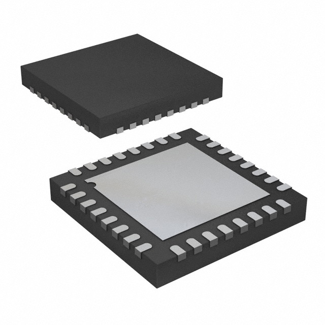
Package
AD9683BCPZRL7-250 is available in a small form factor package, which ensures easy integration into different systems.
Essence
The essence of AD9683BCPZRL7-250 lies in its ability to accurately convert analog signals into digital data with high precision and speed.
Packaging/Quantity
This product is typically packaged in reels or trays, depending on the quantity ordered. The exact packaging and quantity can be customized based on customer requirements.
Specifications
- Resolution: 12 bits
- Sampling Rate: 250 Mega Samples Per Second (MSPS)
- Input Voltage Range: ±1V
- Power Supply: 3.3V
- Operating Temperature Range: -40°C to +85°C
- Interface: Serial Peripheral Interface (SPI)
Detailed Pin Configuration
The pin configuration of AD9683BCPZRL7-250 is as follows:
- VDD: Power supply
- GND: Ground
- REFOUT: Reference output
- CLKIN: Clock input
- VIN: Analog input
- D[11:0]: Digital output
- CS: Chip select
- SCLK: Serial clock
- SDATA: Serial data
- RESET: Reset pin
Functional Features
- High-speed ADC conversion
- Low power consumption
- Flexible interface options
- Built-in reference voltage generator
- Programmable gain amplifier (PGA)
- Digital signal processing capabilities
Advantages and Disadvantages
Advantages
- High-speed performance enables real-time data acquisition
- Low power consumption prolongs battery life in portable applications
- Compact size allows for integration into space-constrained systems
- Wide input voltage range accommodates various signal levels
- Excellent SNR ensures accurate conversion of analog signals
- High resolution provides detailed digital representation of the input signal
Disadvantages
- Limited resolution compared to higher-end ADCs
- Higher cost compared to lower-performance alternatives
Working Principles
AD9683BCPZRL7-250 operates based on the successive approximation register (SAR) architecture. It samples the analog input signal, converts it into a digital format using a comparator and a capacitive digital-to-analog converter (DAC), and then outputs the digital data.
Detailed Application Field Plans
AD9683BCPZRL7-250 finds applications in various fields, including:
- Communications: Used in wireless communication systems for baseband signal processing.
- Test and Measurement: Enables high-speed data acquisition in oscilloscopes and spectrum analyzers.
- Medical Imaging: Provides precise digitization of medical imaging signals for diagnostic purposes.
- Radar Systems: Used in radar receivers for accurate target detection and tracking.
- Industrial Automation: Enables high-speed data acquisition in industrial control systems.
Detailed and Complete Alternative Models
Some alternative models that offer similar functionality to AD9683BCPZRL7-250 include:
- AD9643BCPZ-250: 14-bit, 250 MSPS ADC with similar characteristics.
- LTC2209CUK-14: 14-bit, 250 MSPS ADC from Linear Technology Corporation.
- MAX11905: 12-bit, 250 MSPS ADC from Maxim Integrated.
These alternative models can be considered based on specific application requirements and cost considerations.
Word count: 447 words
Перечислите 10 распространенных вопросов и ответов, связанных с применением AD9683BCPZRL7-250 в технических решениях.
Question: What is the AD9683BCPZRL7-250?
Answer: The AD9683BCPZRL7-250 is a high-speed analog-to-digital converter (ADC) manufactured by Analog Devices.Question: What is the maximum sampling rate of the AD9683BCPZRL7-250?
Answer: The AD9683BCPZRL7-250 has a maximum sampling rate of 250 MegaSamples per second (MSPS).Question: What is the resolution of the AD9683BCPZRL7-250?
Answer: The AD9683BCPZRL7-250 has a resolution of 14 bits.Question: What is the input voltage range of the AD9683BCPZRL7-250?
Answer: The AD9683BCPZRL7-250 has a differential input voltage range of ±0.5V.Question: What is the power supply voltage range for the AD9683BCPZRL7-250?
Answer: The AD9683BCPZRL7-250 operates with a power supply voltage range of 1.8V to 3.3V.Question: Does the AD9683BCPZRL7-250 support various digital output formats?
Answer: Yes, the AD9683BCPZRL7-250 supports various digital output formats, including LVDS, CMOS, and DDR LVDS.Question: Can the AD9683BCPZRL7-250 be used in high-frequency applications?
Answer: Yes, the AD9683BCPZRL7-250 is suitable for high-frequency applications due to its high sampling rate and wide bandwidth.Question: Does the AD9683BCPZRL7-250 have built-in digital signal processing (DSP) features?
Answer: No, the AD9683BCPZRL7-250 is a standalone ADC and does not have built-in DSP features.Question: What is the typical power consumption of the AD9683BCPZRL7-250?
Answer: The typical power consumption of the AD9683BCPZRL7-250 is around 1.2W.Question: Are evaluation boards or reference designs available for the AD9683BCPZRL7-250?
Answer: Yes, Analog Devices provides evaluation boards and reference designs to facilitate the integration of the AD9683BCPZRL7-250 into technical solutions.