

Подробную информацию о продукте см. в характеристиках.
ADP5065ACBZ-1-R7
Product Overview
Category
ADP5065ACBZ-1-R7 belongs to the category of integrated circuits (ICs).
Use
This product is commonly used in electronic devices for power management purposes.
Characteristics
- Integrated circuit
- Power management functionality
- Small form factor
- High efficiency
- Low power consumption
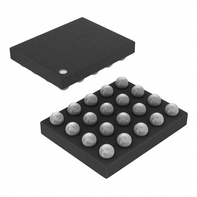
Package
ADP5065ACBZ-1-R7 is available in a compact package, suitable for surface mount technology (SMT) applications.
Essence
The essence of ADP5065ACBZ-1-R7 lies in its ability to efficiently manage power in electronic devices, ensuring optimal performance and energy conservation.
Packaging/Quantity
This product is typically packaged in reels or tubes, with a quantity of 2500 units per reel/tube.
Specifications
- Input Voltage Range: 2.7V to 5.5V
- Output Voltage Range: Programmable from 1.8V to 4.2V
- Maximum Output Current: 500mA
- Quiescent Current: 20µA (typical)
- Operating Temperature Range: -40°C to +85°C
Detailed Pin Configuration
- VIN: Input voltage pin
- GND: Ground pin
- EN: Enable pin
- VOUT: Output voltage pin
- PG: Power good indicator pin
- ISET: Current limit setting pin
- TS: Thermal shutdown pin
Functional Features
- Wide input voltage range allows compatibility with various power sources.
- Programmable output voltage enables flexibility in different applications.
- Power good indicator provides feedback on the status of the output voltage.
- Current limit setting ensures protection against excessive current draw.
- Thermal shutdown feature prevents overheating and damage to the device.
Advantages and Disadvantages
Advantages
- High efficiency power management
- Small form factor for space-constrained applications
- Wide input voltage range for versatility
- Programmable output voltage for flexibility
- Power good indicator for monitoring purposes
Disadvantages
- Limited maximum output current (500mA)
- Quiescent current may be relatively high for ultra-low power applications
Working Principles
ADP5065ACBZ-1-R7 operates based on a switching regulator topology. It takes an input voltage within the specified range and converts it to a programmable output voltage using a control algorithm. The integrated circuit ensures efficient power transfer while providing necessary protection features.
Detailed Application Field Plans
ADP5065ACBZ-1-R7 finds application in various electronic devices, including but not limited to: - Mobile phones - Tablets - Portable media players - Wearable devices - IoT devices
Detailed and Complete Alternative Models
- ADP5066ACBZ-1-R7
- ADP5067ACBZ-1-R7
- ADP5068ACBZ-1-R7
- ADP5069ACBZ-1-R7
- ADP5070ACBZ-1-R7
These alternative models offer similar power management functionality with slight variations in specifications and features.
In conclusion, ADP5065ACBZ-1-R7 is an integrated circuit designed for efficient power management in electronic devices. Its small form factor, wide input voltage range, and programmable output voltage make it suitable for various applications. While it has limitations in terms of maximum output current and quiescent current, it offers several advantages such as high efficiency and a power good indicator.
Перечислите 10 распространенных вопросов и ответов, связанных с применением ADP5065ACBZ-1-R7 в технических решениях.
Sure! Here are 10 common questions and answers related to the application of ADP5065ACBZ-1-R7 in technical solutions:
Q1: What is the ADP5065ACBZ-1-R7? A1: The ADP5065ACBZ-1-R7 is a power management IC (PMIC) designed for use in portable devices, such as smartphones, tablets, and wearables.
Q2: What are the key features of the ADP5065ACBZ-1-R7? A2: Some key features of the ADP5065ACBZ-1-R7 include multiple buck converters, a boost converter, a linear regulator, battery charger, and various protection features.
Q3: What is the input voltage range supported by the ADP5065ACBZ-1-R7? A3: The ADP5065ACBZ-1-R7 supports an input voltage range of 2.8V to 6.0V.
Q4: Can the ADP5065ACBZ-1-R7 charge multiple batteries simultaneously? A4: Yes, the ADP5065ACBZ-1-R7 can charge up to three batteries simultaneously.
Q5: Does the ADP5065ACBZ-1-R7 support fast charging? A5: Yes, the ADP5065ACBZ-1-R7 supports various fast charging protocols, such as USB Power Delivery (USB PD) and Qualcomm Quick Charge.
Q6: What is the maximum charging current supported by the ADP5065ACBZ-1-R7? A6: The ADP5065ACBZ-1-R7 can support a maximum charging current of up to 3A.
Q7: Can the ADP5065ACBZ-1-R7 provide power to the system while charging? A7: Yes, the ADP5065ACBZ-1-R7 can provide power to the system while simultaneously charging the batteries.
Q8: Does the ADP5065ACBZ-1-R7 have any built-in protection features? A8: Yes, the ADP5065ACBZ-1-R7 includes various protection features such as overvoltage protection, overcurrent protection, and thermal shutdown.
Q9: What is the operating temperature range of the ADP5065ACBZ-1-R7? A9: The ADP5065ACBZ-1-R7 has an operating temperature range of -40°C to +85°C.
Q10: Is there any evaluation board available for the ADP5065ACBZ-1-R7? A10: Yes, Analog Devices provides an evaluation board (ADP5065-EVALZ) that allows users to test and evaluate the performance of the ADP5065ACBZ-1-R7 in their applications.
Please note that these answers are general and may vary depending on the specific requirements and implementation of the ADP5065ACBZ-1-R7 in different technical solutions.