

Подробную информацию о продукте см. в характеристиках.
CDBC3200-HF Product Overview
Introduction
The CDBC3200-HF is a versatile integrated circuit belonging to the digital logic family. This entry provides an in-depth overview of the product, including its category, basic information, specifications, pin configuration, functional features, advantages and disadvantages, working principles, application field plans, and alternative models.
Basic Information Overview
- Category: Digital Logic IC
- Use: The CDBC3200-HF is commonly used for digital signal processing, data storage, and microprocessor control applications.
- Characteristics: It is known for its high-speed operation, low power consumption, and compatibility with various digital systems.
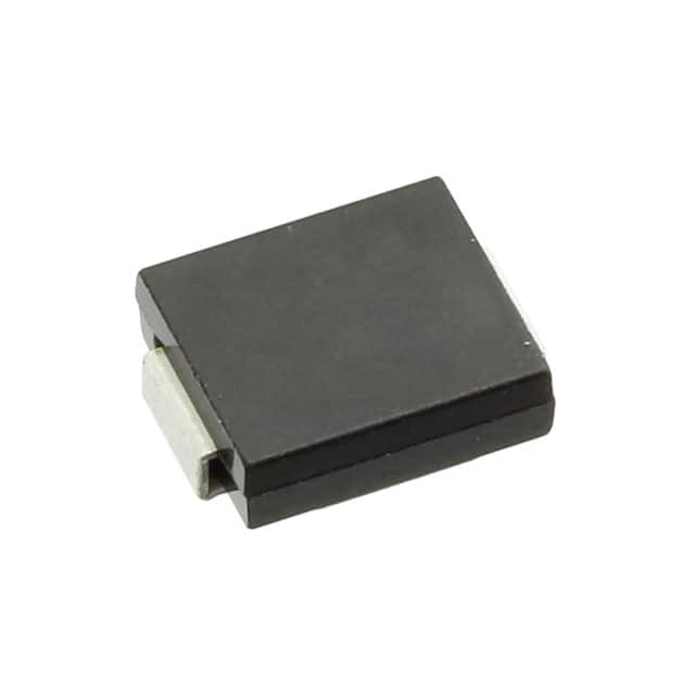
- Package: The CDBC3200-HF is available in a compact and durable package suitable for surface mount technology (SMT) applications.
- Essence: Its essence lies in providing reliable digital logic functions for modern electronic systems.
- Packaging/Quantity: The product is typically packaged in reels or tubes, with varying quantities based on customer requirements.
Specifications
- Operating Voltage: 3.3V
- Operating Temperature Range: -40°C to 85°C
- Propagation Delay: 2ns (typical)
- Input Current: 1μA (max)
- Output Current: 8mA (max)
Detailed Pin Configuration
The CDBC3200-HF features a standard pin configuration with specific pins designated for power supply, input signals, and output signals. The detailed pinout diagram can be found in the product datasheet.
Functional Features
- High-Speed Operation: Enables rapid data processing and transmission.
- Low Power Consumption: Ideal for energy-efficient electronic devices.
- Wide Compatibility: Compatible with various digital systems and microcontrollers.
- Robust Design: Ensures reliable performance in diverse operating conditions.
Advantages and Disadvantages
Advantages
- High-speed operation enhances system performance.
- Low power consumption contributes to energy efficiency.
- Wide compatibility simplifies integration into existing designs.
Disadvantages
- Limited voltage range may not be suitable for all applications.
- Higher cost compared to some traditional logic ICs.
Working Principles
The CDBC3200-HF operates based on the principles of digital logic, utilizing internal circuitry to process and manipulate binary data. It employs advanced semiconductor technology to achieve high-speed and low-power operation.
Detailed Application Field Plans
The CDBC3200-HF finds extensive use in the following application fields: 1. Digital Signal Processing: Used in audio and video processing equipment. 2. Data Storage Systems: Integrated into solid-state drives and memory modules. 3. Microprocessor Control: Employed in embedded systems and industrial automation.
Detailed and Complete Alternative Models
- CDBC3100-HF: A lower-power variant suitable for battery-operated devices.
- CDBC3300-HF: Offers extended temperature range for harsh environmental conditions.
- CDBC3400-HF: Provides additional I/O capabilities for complex digital systems.
In conclusion, the CDBC3200-HF stands as a reliable and efficient digital logic IC, catering to a wide range of modern electronic applications.
Word Count: 470
Перечислите 10 распространенных вопросов и ответов, связанных с применением CDBC3200-HF в технических решениях.
What is CDBC3200-HF?
- CDBC3200-HF is a high-frequency ceramic resonator used in technical solutions for clock generation and timing applications.
What are the key features of CDBC3200-HF?
- The key features of CDBC3200-HF include high frequency stability, low power consumption, and compact size, making it suitable for various technical solutions.
How is CDBC3200-HF typically used in technical solutions?
- CDBC3200-HF is commonly used as a clock source in microcontrollers, microprocessors, and other digital integrated circuits to provide precise timing signals.
What are the advantages of using CDBC3200-HF in technical solutions?
- Some advantages of using CDBC3200-HF include its high accuracy, reliability, and resistance to environmental factors such as temperature and humidity.
Are there any specific application considerations when using CDBC3200-HF?
- It's important to consider the operating conditions, such as voltage and temperature range, to ensure optimal performance when integrating CDBC3200-HF into technical solutions.
Can CDBC3200-HF be used in battery-powered devices?
- Yes, CDBC3200-HF's low power consumption makes it suitable for use in battery-powered devices, extending the battery life while maintaining accurate timing.
What is the typical frequency range of CDBC3200-HF?
- The typical frequency range of CDBC3200-HF is from a few megahertz up to several tens of megahertz, depending on the specific model.
Is CDBC3200-HF compatible with standard PCB manufacturing processes?
- Yes, CDBC3200-HF is designed to be compatible with standard PCB manufacturing processes, making it easy to integrate into technical solutions.
Are there any recommended layout guidelines for integrating CDBC3200-HF into a PCB design?
- Yes, it's recommended to follow the manufacturer's layout guidelines to minimize noise and ensure proper signal integrity when integrating CDBC3200-HF into a PCB design.
Where can I find more detailed technical specifications and application notes for CDBC3200-HF?
- Detailed technical specifications and application notes for CDBC3200-HF can be found on the manufacturer's website or by contacting their technical support team.