

Подробную информацию о продукте см. в характеристиках.
CDBFN140-HF Product Overview
Introduction
The CDBFN140-HF is a versatile integrated circuit that belongs to the category of high-frequency amplifiers. This component is widely used in various electronic applications due to its unique characteristics and functional features.
Basic Information Overview
- Category: High-frequency amplifier IC
- Use: Amplification of high-frequency signals
- Characteristics: High gain, low noise, wide frequency range
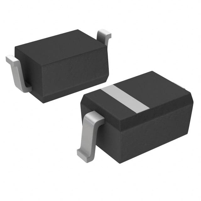
- Package: Small outline package (SOP)
- Essence: Efficient signal amplification
- Packaging/Quantity: Typically supplied in reels of 2500 units
Specifications
- Operating Frequency Range: 1MHz - 2GHz
- Gain: 20dB
- Noise Figure: 2dB
- Supply Voltage: 3.3V
- Current Consumption: 15mA
- Operating Temperature Range: -40°C to 85°C
Detailed Pin Configuration
The CDBFN140-HF features a standard 8-pin small outline package (SOP) with the following pin configuration: 1. VCC 2. RF Input 3. Ground 4. Output 5. Bypass 6. NC (No Connection) 7. NC (No Connection) 8. VCC
Functional Features
- High Gain: Provides significant signal amplification for high-frequency applications.
- Low Noise Figure: Ensures minimal introduction of additional noise during signal amplification.
- Wide Frequency Range: Suitable for amplifying signals across a broad spectrum of frequencies.
Advantages and Disadvantages
Advantages
- High gain for effective signal amplification
- Low noise figure for clean signal amplification
- Wide operating frequency range for versatility
Disadvantages
- Limited to low power applications
- Sensitive to voltage fluctuations
Working Principles
The CDBFN140-HF operates based on the principle of amplifying high-frequency signals using internal transistor configurations. The input signal is amplified with minimal introduction of noise, providing a clean and boosted output signal.
Detailed Application Field Plans
The CDBFN140-HF finds extensive application in the following fields: - Telecommunications - Radio frequency (RF) systems - Wireless communication devices - Radar systems - Test and measurement equipment
Detailed and Complete Alternative Models
For users seeking alternative models, the following integrated circuits can be considered as alternatives to the CDBFN140-HF: 1. CDBFN141-HF 2. CDBFN142-HF 3. CDBFN143-HF
In conclusion, the CDBFN140-HF serves as a reliable high-frequency amplifier IC with its high gain, low noise figure, and wide frequency range, making it suitable for various electronic applications.
Word count: 398
Перечислите 10 распространенных вопросов и ответов, связанных с применением CDBFN140-HF в технических решениях.
What is CDBFN140-HF?
- CDBFN140-HF is a high-frequency ceramic filter used in technical solutions for RF (radio frequency) applications.
What are the key specifications of CDBFN140-HF?
- The key specifications of CDBFN140-HF include its center frequency, bandwidth, insertion loss, and impedance.
How does CDBFN140-HF differ from other filters?
- CDBFN140-HF stands out due to its high-frequency capabilities, low insertion loss, and compact size, making it suitable for demanding RF applications.
In what technical solutions can CDBFN140-HF be used?
- CDBFN140-HF is commonly used in wireless communication systems, radar systems, satellite communication, and other RF-based applications.
What are the advantages of using CDBFN140-HF in technical solutions?
- The advantages of using CDBFN140-HF include its high performance at high frequencies, excellent selectivity, and compact design, which saves space in electronic devices.
How should CDBFN140-HF be integrated into a technical solution?
- CDBFN140-HF should be integrated into the RF circuitry with proper matching networks and shielding to ensure optimal performance and minimal interference.
Can CDBFN140-HF be customized for specific technical requirements?
- Yes, CDBFN140-HF can be customized to meet specific frequency, bandwidth, and impedance requirements for different technical solutions.
What are the temperature and environmental limitations of CDBFN140-HF?
- CDBFN140-HF operates within specified temperature ranges and is designed to withstand typical environmental conditions encountered in technical applications.
Are there any application notes or reference designs available for using CDBFN140-HF?
- Yes, application notes and reference designs are available to guide engineers in implementing CDBFN140-HF in their technical solutions.
Where can I find technical support or further information about CDBFN140-HF?
- Technical support and additional information about CDBFN140-HF can be obtained from the manufacturer's website, datasheets, or by contacting their technical support team directly.