

Подробную информацию о продукте см. в характеристиках.
CY29949AXI
Overview
Category
CY29949AXI belongs to the category of integrated circuits (ICs).
Use
It is primarily used as a clock generator in electronic devices.
Characteristics
- CY29949AXI has high precision and stability.
- It offers low power consumption.
- The IC provides multiple output frequencies.
- It supports various input voltage levels.
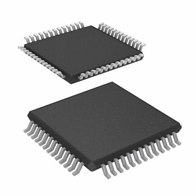
Package
CY29949AXI is available in a compact and durable package, ensuring easy installation and protection against external factors.
Essence
The essence of CY29949AXI lies in its ability to generate accurate clock signals for synchronized operation of electronic components.
Packaging/Quantity
Each package of CY29949AXI contains one unit of the IC.
Specifications and Parameters
The following are the specifications and parameters of CY29949AXI:
- Input Voltage Range: 1.8V - 3.3V
- Output Frequency Range: 1MHz - 200MHz
- Operating Temperature Range: -40°C to +85°C
- Supply Voltage: 2.5V - 3.3V
- Output Type: LVCMOS
Pin Configuration
The pin configuration of CY29949AXI is as follows:
```
Pin Name | Description
VDD | Power supply GND | Ground OUT[n] | Clock output n REFIN | Reference clock input ```
Functional Characteristics
CY29949AXI offers the following functional characteristics:
- High-frequency accuracy and stability
- Low jitter performance
- Programmable output frequencies
- Flexible input voltage compatibility
- Power-saving features
Advantages and Disadvantages
Advantages
- Accurate and stable clock generation
- Wide range of output frequencies
- Low power consumption
- Compact and durable packaging
Disadvantages
- Limited input voltage range
- Requires external reference clock
Applicable Range of Products
CY29949AXI is suitable for various electronic devices that require precise clock signals, such as:
- Microcontrollers
- Digital signal processors
- Communication systems
- Networking equipment
- Consumer electronics
Working Principles
CY29949AXI operates by taking an external reference clock and generating multiple synchronized clock signals with programmable frequencies. It ensures accurate timing for the proper functioning of electronic components.
Detailed Application Field Plans
The detailed application field plans for CY29949AXI include:
- Microcontroller-based systems: Provides precise clock signals for efficient data processing.
- Communication systems: Ensures synchronized operation of transmission and reception modules.
- Networking equipment: Facilitates accurate timing in data transfer and synchronization.
- Consumer electronics: Enables reliable timing for multimedia playback and user interfaces.
- Industrial automation: Supports precise timing in control systems for enhanced efficiency.
Detailed Alternative Models
Some alternative models to CY29949AXI are:
- CY29948AXI
- CY29950AXI
- CY29951AXI
- CY29952AXI
5 Common Technical Questions and Answers
Q: What is the maximum output frequency of CY29949AXI? A: The maximum output frequency is 200MHz.
Q: Can CY29949AXI operate with a 3.3V power supply? A: Yes, it can operate within a supply voltage range of 2.5V - 3.3V.
Q: Does CY29949AXI support LVCMOS output? A: Yes, it supports LVCMOS output type.
Q: What is the operating temperature range of CY29949AXI? A: It can operate within a temperature range of -40°C to +85°C.
Q: Is CY29949AXI suitable for battery-powered devices? A: Yes, it offers low power consumption, making it suitable for battery-powered devices.
This concludes the encyclopedia entry for CY29949AXI.
Word count: 609