

Подробную информацию о продукте см. в характеристиках.
Encyclopedia Entry: 74AUP1G32FS3-7
Product Overview
Category
The 74AUP1G32FS3-7 belongs to the category of integrated circuits (ICs), specifically logic gates.
Use
This product is commonly used in digital electronics for logical operations, specifically as a 2-input OR gate.
Characteristics
- Low power consumption
- High-speed operation
- Wide operating voltage range
- Small package size
- RoHS compliant
Package and Quantity
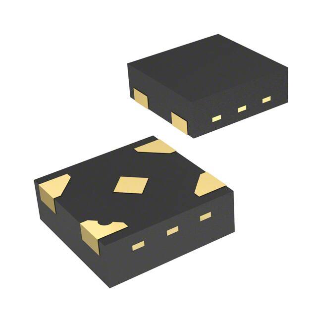
The 74AUP1G32FS3-7 is available in a small surface-mount package, such as SOT353 or SC-88. It is typically sold in reels or tubes containing multiple units.
Essence
The essence of the 74AUP1G32FS3-7 lies in its ability to perform logical OR operations with two input signals, providing a single output signal based on the logical combination of the inputs.
Specifications
- Supply Voltage Range: 0.8V to 3.6V
- Input Voltage Range: 0V to VCC
- Output Voltage Range: 0V to VCC
- Operating Temperature Range: -40°C to +85°C
- Propagation Delay: <5ns
- Maximum Quiescent Current: 10μA
Detailed Pin Configuration
The 74AUP1G32FS3-7 has a total of five pins: 1. GND (Ground) 2. A (Input A) 3. B (Input B) 4. Y (Output) 5. VCC (Supply Voltage)
Functional Features
- Logical OR operation: The 74AUP1G32FS3-7 performs a logical OR operation on the input signals A and B, producing an output signal Y.
- High-speed operation: This IC operates at high speeds, making it suitable for applications requiring quick response times.
- Low power consumption: The 74AUP1G32FS3-7 is designed to minimize power consumption, making it ideal for battery-powered devices.
Advantages and Disadvantages
Advantages
- Low power consumption extends battery life in portable devices.
- High-speed operation allows for efficient data processing.
- Wide operating voltage range enables compatibility with various systems.
- Small package size saves board space in compact designs.
Disadvantages
- Limited to 2-input OR gate functionality.
- May not be suitable for complex logic operations requiring multiple gates.
Working Principles
The 74AUP1G32FS3-7 operates based on the principles of Boolean logic. It combines the input signals A and B using an internal circuit to generate the output signal Y. When either input A or B (or both) is high, the output Y will be high. Otherwise, the output will be low.
Detailed Application Field Plans
The 74AUP1G32FS3-7 finds applications in various digital systems, including: - Consumer electronics - Mobile devices - Industrial automation - Automotive electronics - Communication systems
Alternative Models
Other alternative models that provide similar functionality to the 74AUP1G32FS3-7 include: - SN74LVC1G32DBVR - MC74VHC1G32DTT1G - TC7SZ32FU
These alternatives can be considered based on specific requirements, such as voltage range, speed, and package type.
In conclusion, the 74AUP1G32FS3-7 is a versatile logic gate IC that offers low power consumption, high-speed operation, and wide voltage range. Its small package size makes it suitable for compact designs in various application fields. However, its limited functionality as a 2-input OR gate may require alternative models for more complex logic operations.
Перечислите 10 распространенных вопросов и ответов, связанных с применением 74AUP1G32FS3-7 в технических решениях.
Sure! Here are 10 common questions and answers related to the application of the 74AUP1G32FS3-7 in technical solutions:
Q1: What is the 74AUP1G32FS3-7? A1: The 74AUP1G32FS3-7 is a single 2-input OR gate with Schmitt-trigger inputs. It is a commonly used integrated circuit (IC) in digital logic circuits.
Q2: What is the operating voltage range of the 74AUP1G32FS3-7? A2: The operating voltage range of the 74AUP1G32FS3-7 is from 0.8V to 3.6V.
Q3: What is the maximum output current of the 74AUP1G32FS3-7? A3: The maximum output current of the 74AUP1G32FS3-7 is 32mA.
Q4: Can the 74AUP1G32FS3-7 be used in battery-powered applications? A4: Yes, the 74AUP1G32FS3-7 can be used in battery-powered applications as it operates within a low voltage range.
Q5: What is the propagation delay of the 74AUP1G32FS3-7? A5: The propagation delay of the 74AUP1G32FS3-7 is typically around 2.5ns.
Q6: Can the 74AUP1G32FS3-7 be used in high-speed applications? A6: Yes, the 74AUP1G32FS3-7 can be used in high-speed applications due to its low propagation delay.
Q7: Is the 74AUP1G32FS3-7 compatible with other logic families? A7: Yes, the 74AUP1G32FS3-7 is compatible with a wide range of logic families, including TTL and CMOS.
Q8: Can the 74AUP1G32FS3-7 be used in both digital and analog circuits? A8: No, the 74AUP1G32FS3-7 is specifically designed for digital logic applications and may not perform optimally in analog circuits.
Q9: What is the package type of the 74AUP1G32FS3-7? A9: The 74AUP1G32FS3-7 is available in a small SOT353 package.
Q10: Are there any recommended operating conditions for the 74AUP1G32FS3-7? A10: Yes, some recommended operating conditions include a supply voltage between 0.8V and 3.6V, an ambient temperature range of -40°C to +85°C, and proper decoupling capacitors for stable operation.
Please note that these answers are general and it's always recommended to refer to the datasheet and application notes provided by the manufacturer for specific details and guidelines.