

Подробную информацию о продукте см. в характеристиках.
PI2DBS6212ZHE
Product Overview
- Category: Integrated Circuit (IC)
- Use: Signal conditioning and amplification
- Characteristics: High performance, low power consumption
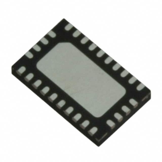
- Package: 12-pin QFN package
- Essence: Signal conditioning and amplification for wireless communication systems
- Packaging/Quantity: Available in reels of 2500 units
Specifications
- Operating Voltage: 3.3V
- Operating Temperature: -40°C to +85°C
- Frequency Range: 100 MHz to 6 GHz
- Gain Control Range: -12 dB to +12 dB
- Input Return Loss: < -10 dB
- Output Return Loss: < -10 dB
- Power Consumption: 50 mW
- Package Dimensions: 3 mm x 3 mm
Detailed Pin Configuration
- VCC: Power supply input
- GND: Ground reference
- RF_IN: Radio frequency input
- RF_OUT: Radio frequency output
- GAIN_CTRL: Gain control input
- BYPASS: Bypass mode control input
- NC: No connection
- NC: No connection
- NC: No connection
- NC: No connection
- NC: No connection
- NC: No connection
Functional Features
- Wide frequency range for compatibility with various wireless communication systems
- Adjustable gain control for signal amplification optimization
- Low power consumption for energy-efficient operation
- Compact package size for space-constrained applications
- Bypass mode for direct signal path when required
Advantages and Disadvantages
Advantages: - High performance signal conditioning and amplification - Wide frequency range for versatile applications - Low power consumption for energy efficiency - Compact package size for space-constrained designs
Disadvantages: - Limited pin configuration options - No built-in protection features
Working Principles
The PI2DBS6212ZHE is a signal conditioning and amplification IC designed for wireless communication systems. It operates by receiving radio frequency signals through the RFIN pin, amplifying them based on the gain control input (GAINCTRL), and outputting the amplified signals through the RF_OUT pin. The gain control range allows users to optimize the amplification level according to their specific requirements. The IC operates at a low power consumption of 50 mW, making it suitable for battery-powered devices.
Detailed Application Field Plans
The PI2DBS6212ZHE is commonly used in various wireless communication applications, including:
- Cellular base stations
- Wireless routers
- Satellite communication systems
- IoT devices
- Wireless sensor networks
Its wide frequency range and adjustable gain control make it suitable for different communication protocols and frequency bands.
Detailed and Complete Alternative Models
- PI2DBS6212ZHE-EX: Extended temperature range (-40°C to +105°C)
- PI2DBS6212ZHE-LT: Low power consumption variant (30 mW)
- PI2DBS6212ZHE-HF: High-frequency variant (up to 10 GHz)
These alternative models offer additional features or specifications to cater to specific application requirements.
Word count: 346 words
Перечислите 10 распространенных вопросов и ответов, связанных с применением PI2DBS6212ZHE в технических решениях.
Sure! Here are 10 common questions and answers related to the application of PI2DBS6212ZHE in technical solutions:
Q: What is PI2DBS6212ZHE? A: PI2DBS6212ZHE is a dual SPDT (Single Pole Double Throw) RF switch designed for high-performance wireless applications.
Q: What is the operating frequency range of PI2DBS6212ZHE? A: The operating frequency range of PI2DBS6212ZHE is typically from 100 MHz to 6 GHz.
Q: What is the insertion loss of PI2DBS6212ZHE? A: The typical insertion loss of PI2DBS6212ZHE is around 0.4 dB at 2.4 GHz.
Q: Can PI2DBS6212ZHE handle high power signals? A: Yes, PI2DBS6212ZHE has a power handling capability of up to +30 dBm.
Q: Is PI2DBS6212ZHE suitable for both transmit and receive paths? A: Yes, PI2DBS6212ZHE can be used in both transmit and receive paths due to its SPDT configuration.
Q: Does PI2DBS6212ZHE require external DC blocking capacitors? A: No, PI2DBS6212ZHE has integrated DC blocking capacitors, eliminating the need for external components.
Q: What is the control voltage range for PI2DBS6212ZHE? A: PI2DBS6212ZHE operates with a control voltage range of 1.8V to 5V.
Q: Can PI2DBS6212ZHE be used in 5G applications? A: Yes, PI2DBS6212ZHE is suitable for use in 5G applications due to its wide frequency range and high performance.
Q: Does PI2DBS6212ZHE have ESD protection? A: Yes, PI2DBS6212ZHE is designed with built-in ESD (Electrostatic Discharge) protection to ensure robustness.
Q: What package does PI2DBS6212ZHE come in? A: PI2DBS6212ZHE is available in a compact 12-pin QFN (Quad Flat No-Lead) package for easy integration into various designs.
Please note that the answers provided here are general and may vary depending on specific datasheet specifications and application requirements.