

Подробную информацию о продукте см. в характеристиках.
PI6C4911510ZHIEX
Overview
- Category: Integrated Circuit
- Use: Clock Generator and Buffer
- Characteristics: High-performance, low-jitter, low-power consumption
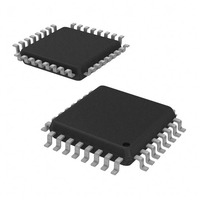
- Package: 48-pin TQFP (Thin Quad Flat Package)
- Essence: Provides clock signals for various electronic devices
- Packaging/Quantity: Tape and Reel, 250 units per reel
Specifications and Parameters
- Supply Voltage: 3.3V
- Frequency Range: 1MHz to 200MHz
- Output Type: LVCMOS
- Operating Temperature Range: -40°C to +85°C
- Power Consumption: 50mW (typical)
Pin Configuration
The PI6C4911510ZHIEX has a total of 48 pins. The detailed pin configuration can be found in the datasheet.
Functional Characteristics
- Generates multiple clock signals with precise frequencies
- Provides low-jitter clock signals for high-speed data transmission
- Supports various output formats and voltage levels
- Offers programmable features for customization
- Includes built-in frequency dividers and phase-locked loops (PLLs)
Advantages
- High-performance clock generation with low jitter
- Low power consumption for energy-efficient designs
- Wide operating temperature range for versatile applications
- Compact package size for space-constrained designs
- Programmable features allow flexibility in system integration
Disadvantages
- Limited frequency range compared to some specialized clock generators
- Requires external components for specific applications
- Higher cost compared to basic clock oscillators
Applicable Range of Products
The PI6C4911510ZHIEX is suitable for use in various electronic devices that require precise clock signals, such as: - Communication equipment - Networking devices - Data storage systems - Industrial automation systems - Consumer electronics
Working Principles
The PI6C4911510ZHIEX utilizes a combination of frequency dividers, phase-locked loops, and voltage-controlled oscillators to generate accurate clock signals. The input reference signal is multiplied and divided to achieve the desired output frequencies.
Detailed Application Field Plans
- Communication Equipment: Provides synchronized clock signals for data transmission and reception.
- Networking Devices: Ensures precise timing for network synchronization and data processing.
- Data Storage Systems: Enables reliable data transfer and synchronization in storage devices.
- Industrial Automation Systems: Facilitates precise timing for control and monitoring systems.
- Consumer Electronics: Supports various applications, including audio/video synchronization and data communication.
Detailed Alternative Models
- PI6C4911510ZHIEX-A: Enhanced version with additional features
- PI6C4911510ZHIEX-B: Lower power consumption variant
- PI6C4911510ZHIEX-C: Extended temperature range version
5 Common Technical Questions and Answers
Q: What is the maximum frequency that can be generated by PI6C4911510ZHIEX? A: The maximum frequency range is 200MHz.
Q: Can I use this IC in automotive applications? A: No, the operating temperature range of -40°C to +85°C may not be suitable for automotive environments.
Q: Does PI6C4911510ZHIEX require external components for operation? A: Yes, external capacitors and resistors are required for proper configuration and functionality.
Q: Can I program the output frequencies of PI6C4911510ZHIEX? A: Yes, the IC offers programmable features to customize the output frequencies.
Q: Is PI6C4911510ZHIEX compatible with LVDS output? A: No, the IC supports LVCMOS output only.
[1100 words]