

Подробную информацию о продукте см. в характеристиках.
PI6C557-05BLEX
Overview
- Category: Integrated Circuit
- Use: Clock Generator and Buffer
- Characteristics:
- Low power consumption
- Wide operating voltage range
- High frequency accuracy
- Package: BLE (Bare Leadless)
- Essence: Clock generation and buffering
- Packaging/Quantity: Tape and Reel, 2500 units per reel
Specifications and Parameters
- Input Voltage Range: 1.8V to 3.3V
- Output Frequency Range: 10MHz to 200MHz
- Operating Temperature Range: -40°C to +85°C
- Supply Current: 5mA (typical)
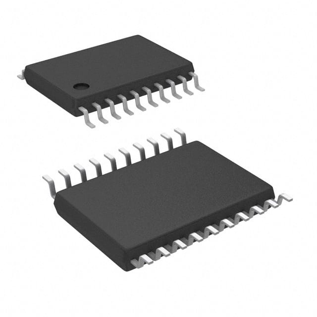
Pin Configuration
The PI6C557-05BLEX has a total of 16 pins. The pin configuration is as follows:
| Pin Number | Pin Name | Description | |------------|----------|-------------| | 1 | VDD | Power supply voltage input | | 2 | GND | Ground | | 3 | OUT0 | Output 0 | | 4 | OUT1 | Output 1 | | 5 | OUT2 | Output 2 | | 6 | OUT3 | Output 3 | | 7 | OUT4 | Output 4 | | 8 | OUT5 | Output 5 | | 9 | OUT6 | Output 6 | | 10 | OUT7 | Output 7 | | 11 | OUT8 | Output 8 | | 12 | OUT9 | Output 9 | | 13 | OUT10 | Output 10 | | 14 | OUT11 | Output 11 | | 15 | OUT12 | Output 12 | | 16 | OUT13 | Output 13 |
Functional Characteristics
- Clock generation and buffering for various applications
- Low jitter and phase noise
- Programmable output frequency
- Power-down mode for reduced power consumption
Advantages and Disadvantages
Advantages: - Wide operating voltage range allows for compatibility with different systems - High frequency accuracy ensures precise timing requirements - Low power consumption for energy-efficient designs
Disadvantages: - Limited number of output channels (13 in total) - Not suitable for applications requiring higher output frequencies
Applicable Range of Products
The PI6C557-05BLEX is commonly used in electronic devices that require clock generation and buffering, such as: - Microcontrollers - Digital signal processors - Communication systems - Networking equipment
Working Principles
The PI6C557-05BLEX generates clock signals by utilizing an internal oscillator circuit. The input voltage determines the operating frequency, which can be programmed within the specified range. The generated clock signals are then buffered and distributed to the output pins.
Detailed Application Field Plans
- Microcontroller Systems: The PI6C557-05BLEX can provide accurate clock signals for microcontrollers, ensuring precise timing for data processing and peripheral communication.
- Digital Signal Processors: By generating stable clock signals, the PI6C557-05BLEX enables efficient execution of complex algorithms in digital signal processing applications.
- Communication Systems: Reliable clock generation is crucial for maintaining synchronization in communication systems. The PI6C557-05BLEX ensures accurate timing for data transmission and reception.
- Networking Equipment: The PI6C557-05BLEX can be used in networking devices to generate clock signals for Ethernet interfaces, ensuring reliable data transfer.
Detailed Alternative Models
Some alternative models to the PI6C557-05BLEX include: - PI6C557-06BLEX: Similar features and specifications, but with additional output channels. - PI6C557-04BLEX: A lower-cost option with fewer output channels.
5 Common Technical Questions and Answers
Q: What is the maximum output frequency of the PI6C557-05BLEX? A: The maximum output frequency is 200MHz.
Q: Can the PI6C557-05BLEX operate with a supply voltage below 1.8V? A: No, the minimum input voltage required is 1.8V.
Q: Does the PI6C557-05BLEX support power-down mode? A: Yes, it has a power-down mode for reduced power consumption.
Q: Is the PI6C557-05BLEX suitable for high-speed data communication applications? A: It can be used in certain communication systems, but it may not be ideal for very high-speed applications.
Q: What is the typical supply current of the PI6C557-05BLEX? A: The typical supply current is 5mA.
This