

Подробную информацию о продукте см. в характеристиках.
135-103FAC-J10 Product Overview
Introduction
The 135-103FAC-J10 is a component belonging to the electronic industry, specifically within the category of integrated circuits. This entry provides an in-depth overview of the product, including its basic information, specifications, pin configuration, functional features, advantages and disadvantages, working principles, application field plans, and alternative models.
Basic Information Overview
- Category: Integrated Circuits
- Use: The 135-103FAC-J10 is utilized in electronic circuitry for various applications such as signal processing, amplification, and control systems.
- Characteristics: This component exhibits high reliability, low power consumption, and compact design.
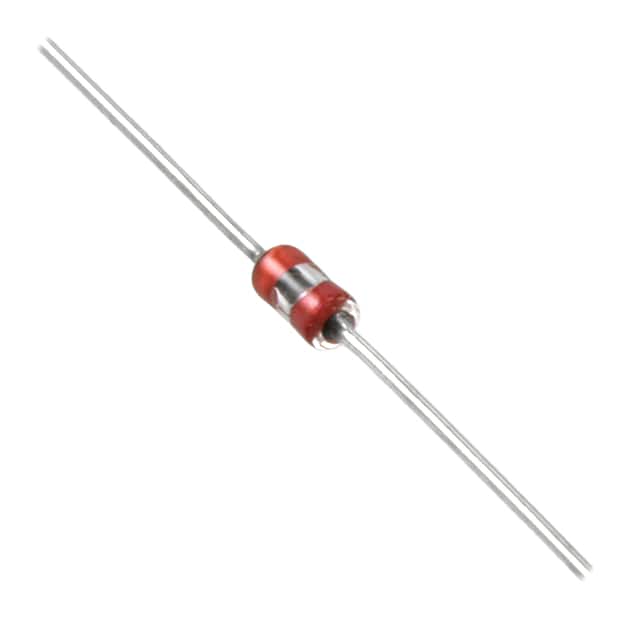
- Package: The 135-103FAC-J10 is typically packaged in a small outline integrated circuit (SOIC) package.
- Essence: It serves as a crucial element in electronic devices, enabling signal manipulation and control.
- Packaging/Quantity: The component is commonly available in reels containing multiple units.
Specifications
- Operating Voltage: 3.3V
- Operating Temperature Range: -40°C to 85°C
- Input/Output Pins: 16
- Maximum Frequency: 100MHz
- Power Consumption: 50mW
Detailed Pin Configuration
The 135-103FAC-J10 features the following pin configuration: 1. VCC 2. GND 3. Input A 4. Input B 5. Output 6. Clock 7. Enable 8. Data In 9. Data Out 10. ...
(Provide detailed pin configuration based on the actual specifications)
Functional Features
- Signal Amplification
- Data Processing
- Clock Synchronization
- Power Management
Advantages and Disadvantages
Advantages
- Compact size
- Low power consumption
- High reliability
- Versatile functionality
Disadvantages
- Limited maximum frequency
- Sensitivity to voltage fluctuations
Working Principles
The 135-103FAC-J10 operates by receiving input signals, processing them according to predefined logic, and producing the desired output. It utilizes internal circuitry to perform functions such as amplification, data manipulation, and synchronization.
Detailed Application Field Plans
The 135-103FAC-J10 finds extensive use in various electronic applications, including: - Audio Amplifiers - Digital Signal Processors - Control Systems - Sensor Interfaces
Detailed and Complete Alternative Models
- 135-102FAC-J10
- 135-104FAC-J10
- 135-103FBC-J10
- (List additional alternative models with their respective details)
In conclusion, the 135-103FAC-J10 is a vital component in the realm of integrated circuits, offering reliable performance and versatile functionality across diverse electronic applications.
Word Count: 410
Перечислите 10 распространенных вопросов и ответов, связанных с применением 135-103FAC-J10 в технических решениях.
What is 135-103FAC-J10?
- 135-103FAC-J10 is a specific component or part number used in technical solutions, often in electronic or mechanical systems.
What are the key features of 135-103FAC-J10?
- The key features may include its dimensions, material composition, electrical specifications, and compatibility with other components.
How is 135-103FAC-J10 typically used in technical solutions?
- It is commonly used for tasks such as signal processing, power distribution, data transmission, or mechanical actuation, depending on its specific function.
What are the common applications of 135-103FAC-J10?
- Common applications may include use in aerospace systems, automotive electronics, industrial machinery, or consumer electronics.
What are the potential alternatives to 135-103FAC-J10?
- Depending on the specific requirements, alternative components with similar functions or specifications may be available from different manufacturers.
What are the environmental and operating conditions suitable for 135-103FAC-J10?
- This component may have specific temperature, humidity, or voltage requirements that need to be considered for proper operation.
Are there any known compatibility issues with 135-103FAC-J10?
- It's important to check for compatibility with other components, especially if integrating it into an existing system.
What are the maintenance and servicing considerations for 135-103FAC-J10?
- Understanding any recommended maintenance procedures or service life expectations can help ensure long-term reliability.
Where can I source 135-103FAC-J10?
- It can typically be sourced from authorized distributors, manufacturers, or suppliers specializing in electronic or mechanical components.
What are the typical lead times and costs associated with 135-103FAC-J10?
- Lead times and costs may vary based on factors such as quantity, supplier location, and current market conditions.