

Подробную информацию о продукте см. в характеристиках.
Encyclopedia Entry: 54FCT374TDB
Product Overview
Category
The 54FCT374TDB belongs to the category of integrated circuits (ICs) and specifically falls under the family of flip-flops.
Use
This IC is primarily used for storing and transferring digital data in electronic systems. It serves as a latch or register, allowing the storage and retrieval of binary information.
Characteristics
- The 54FCT374TDB operates on a supply voltage range of 4.5V to 5.5V.
- It offers high-speed performance, making it suitable for applications requiring quick data transfer.
- This IC has a wide operating temperature range, typically from -40°C to +85°C, ensuring its functionality in various environments.
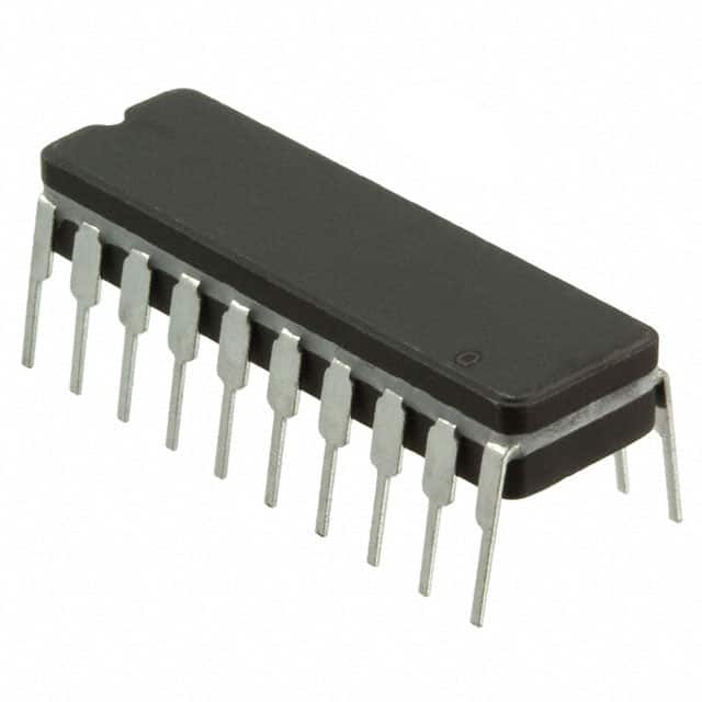
Package
The 54FCT374TDB is available in a standard 20-pin dual in-line package (DIP), which facilitates easy integration into circuit boards.
Essence
The essence of the 54FCT374TDB lies in its ability to store and manipulate digital data efficiently, enabling seamless data flow within electronic systems.
Packaging/Quantity
This IC is commonly packaged in reels or tubes, with each reel containing approximately 250 units.
Specifications
- Supply Voltage Range: 4.5V to 5.5V
- Operating Temperature Range: -40°C to +85°C
- Package Type: 20-pin DIP
- Logic Family: 54FCT
- Flip-Flop Type: D-type (Latch)
- Output Type: Tri-state
Detailed Pin Configuration
The 54FCT374TDB features a total of 20 pins, each serving a specific purpose. Here is the detailed pin configuration:
- Pin 1: Data Input (D0)
- Pin 2: Data Input (D1)
- Pin 3: Data Input (D2)
- Pin 4: Data Input (D3)
- Pin 5: Data Input (D4)
- Pin 6: Data Input (D5)
- Pin 7: Data Input (D6)
- Pin 8: Data Input (D7)
- Pin 9: Clock Input (CLK)
- Pin 10: Output Enable (OE)
- Pin 11: Master Reset (MR)
- Pin 12: Q0 Output
- Pin 13: Q1 Output
- Pin 14: Q2 Output
- Pin 15: Q3 Output
- Pin 16: Q4 Output
- Pin 17: Q5 Output
- Pin 18: Q6 Output
- Pin 19: Q7 Output
- Pin 20: Ground (GND)
Functional Features
The 54FCT374TDB offers the following functional features:
- Data Storage: It can store data inputs on the rising edge of the clock signal.
- Tri-State Outputs: The outputs can be put in a high-impedance state using the output enable pin, allowing multiple devices to share a common bus.
- Master Reset: The master reset pin resets all flip-flops to their initial state when activated.
Advantages and Disadvantages
Advantages
- High-speed operation enables efficient data transfer.
- Tri-state outputs facilitate bus sharing among multiple devices.
- Wide operating temperature range ensures versatility in various environments.
Disadvantages
- Limited voltage supply range restricts compatibility with certain systems.
- The DIP package may not be suitable for space-constrained applications.
Working Principles
The 54FCT374TDB operates based on the principles of sequential logic. It utilizes flip-flops to store and transfer digital data. The clock signal triggers the storage of input data, while the output enable pin controls the output state. The master reset pin allows for resetting all flip-flops simultaneously.
Detailed Application Field Plans
The 54FCT374TDB finds applications in various electronic systems, including but not limited to: - Microprocessors and microcontrollers - Data storage devices - Communication systems - Digital signal processing - Industrial automation
Detailed and Complete Alternative Models
Here are some alternative models that offer similar functionality to the 54FCT374TDB: - 74HC374: A CMOS-based octal D-type flip-flop with tri-state outputs. - CD4013: Dual D-type flip-flop with complementary outputs. - SN74LS374: Octal D-type flip-flop with tri-state outputs.
These alternatives provide options based on different logic families and package types, allowing flexibility in design choices.
In conclusion, the 54FCT374TDB is a versatile integrated circuit used for storing and transferring digital data. Its high-speed operation, tri-state outputs, and wide temperature range make it
Перечислите 10 распространенных вопросов и ответов, связанных с применением 54FCT374TDB в технических решениях.
Sure! Here are 10 common questions and answers related to the application of 54FCT374TDB in technical solutions:
Q: What is the 54FCT374TDB? A: The 54FCT374TDB is a type of octal D-type flip-flop integrated circuit (IC) that can store and transfer data in digital systems.
Q: What is the purpose of using the 54FCT374TDB in technical solutions? A: The 54FCT374TDB is commonly used for data storage, synchronization, and signal buffering in various digital applications.
Q: How many flip-flops are there in the 54FCT374TDB? A: The 54FCT374TDB consists of eight individual D-type flip-flops, making it an octal flip-flop IC.
Q: What is the maximum operating frequency of the 54FCT374TDB? A: The maximum operating frequency of the 54FCT374TDB is typically specified by the manufacturer and can vary, but it is commonly in the range of several hundred megahertz (MHz).
Q: Can the 54FCT374TDB be used in both synchronous and asynchronous applications? A: Yes, the 54FCT374TDB can be used in both synchronous and asynchronous applications, depending on the specific requirements of the system.
Q: What is the power supply voltage range for the 54FCT374TDB? A: The power supply voltage range for the 54FCT374TDB is typically specified by the manufacturer and can vary, but it is commonly in the range of 4.5V to 5.5V.
Q: Does the 54FCT374TDB have any special features or additional functionality? A: The 54FCT374TDB is a basic flip-flop IC and does not have any special features or additional functionality beyond its core operation.
Q: Can the 54FCT374TDB be cascaded to increase the number of flip-flops in a system? A: Yes, multiple 54FCT374TDB ICs can be cascaded together to increase the number of flip-flops in a system, allowing for larger data storage capabilities.
Q: What are the typical input and output voltage levels for the 54FCT374TDB? A: The typical input voltage levels for the 54FCT374TDB are based on the power supply voltage range and can vary, but they are commonly compatible with standard logic levels (e.g., TTL or CMOS). The output voltage levels are typically determined by the power supply voltage.
Q: Are there any specific considerations or precautions when using the 54FCT374TDB in technical solutions? A: It is important to follow the manufacturer's datasheet and guidelines for proper usage, including considerations such as power supply decoupling, signal integrity, and temperature limitations. Additionally, it is recommended to handle the IC with appropriate electrostatic discharge (ESD) precautions to prevent damage.