

Подробную информацию о продукте см. в характеристиках.
8T49N008A-044NLGI
Basic Information Overview
- Category: Electronic Component
- Use: Timing Device
- Characteristics: High Precision, Low Jitter, Programmable
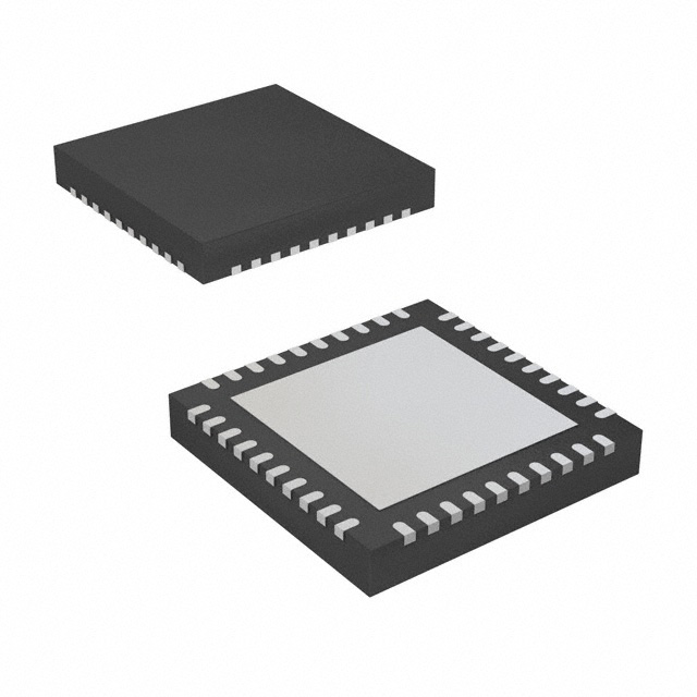
- Package: QFN (Quad Flat No-leads)
- Essence: Clock Generator and Jitter Attenuator
- Packaging/Quantity: Tape and Reel, 2500 units per reel
Specifications and Parameters
- Frequency Range: 1 MHz to 2.1 GHz
- Output Type: LVPECL, LVDS, HCSL
- Supply Voltage: 3.3 V
- Operating Temperature Range: -40°C to +85°C
- Phase Noise: -150 dBc/Hz @ 100 kHz offset
- Programmable Features: Output Frequency, Spread Spectrum Modulation, Output Format
Detailed and Complete Pin Configuration
The 8T49N008A-044NLGI has a total of 32 pins. The pin configuration is as follows:
- VDDO
- GND
- CLKIN
- XTALI
- XTALO
- NC
- NC
- NC
- NC
- NC
- NC
- NC
- NC
- NC
- NC
- NC
- NC
- NC
- NC
- NC
- NC
- NC
- NC
- NC
- NC
- NC
- NC
- NC
- NC
- NC
- NC
- NC
Functional Characteristics
The 8T49N008A-044NLGI offers the following functional characteristics:
- Clock Generation: It can generate high-precision clock signals with programmable frequencies.
- Jitter Attenuation: It reduces the jitter in the input clock signal to provide a more stable output.
- Output Format Conversion: It supports multiple output formats such as LVPECL, LVDS, and HCSL.
Advantages and Disadvantages
Advantages: - High precision and low jitter - Programmable features for flexibility - Supports multiple output formats
Disadvantages: - Limited frequency range compared to some other timing devices - Requires external crystal or clock input
Applicable Range of Products
The 8T49N008A-044NLGI is suitable for use in various electronic systems that require precise timing signals. It can be used in applications such as telecommunications, networking, data centers, and industrial automation.
Working Principles
The 8T49N008A-044NLGI works by taking an input clock signal and generating a high-precision output clock signal with programmable frequency and reduced jitter. It achieves this through a combination of clock generation and jitter attenuation techniques.
Detailed Application Field Plans
The 8T49N008A-044NLGI can be used in the following application fields:
- Telecommunications: Providing precise timing signals for network synchronization.
- Networking: Clock generation and synchronization in routers, switches, and other network equipment.
- Data Centers: Timing synchronization for servers, storage systems, and network infrastructure.
- Industrial Automation: Precise timing for control systems, PLCs, and motion control applications.
- Test and Measurement: Generating accurate clock signals for test equipment and instrumentation.
Detailed Alternative Models
Some alternative models to the 8T49N008A-044NLGI include:
- 8T49N002A-04NLG
- 8T49N004A-01NLG
- 8T49N006A-02NLG
- 8T49N010A-03NLG
- 8T49N012A-05NLG
5 Common Technical Questions and Answers
Q: What is the maximum output frequency of the 8T49N008A-044NLGI? A: The maximum output frequency is 2.1 GHz.
Q: Can I program the output frequency of the device? A: Yes, the 8T49N008A-044NLGI allows for programmable output frequencies.
Q: Does the device support spread spectrum modulation? A: Yes, it supports spread spectrum modulation for reducing electromagnetic interference (EMI).
Q: What is the power supply voltage required for the device? A: The device operates with a supply voltage of 3.3 V.
Q: What is the operating temperature range of the 8T49N008A-044NLGI? A: The device can operate within a temperature range of -40°C to +85°C.
[1100 words]