

Подробную информацию о продукте см. в характеристиках.
IPI60R165CPAKSA1
Product Overview
- Category: Power MOSFET
- Use: Power switching applications
- Characteristics: High voltage, low on-resistance, fast switching speed
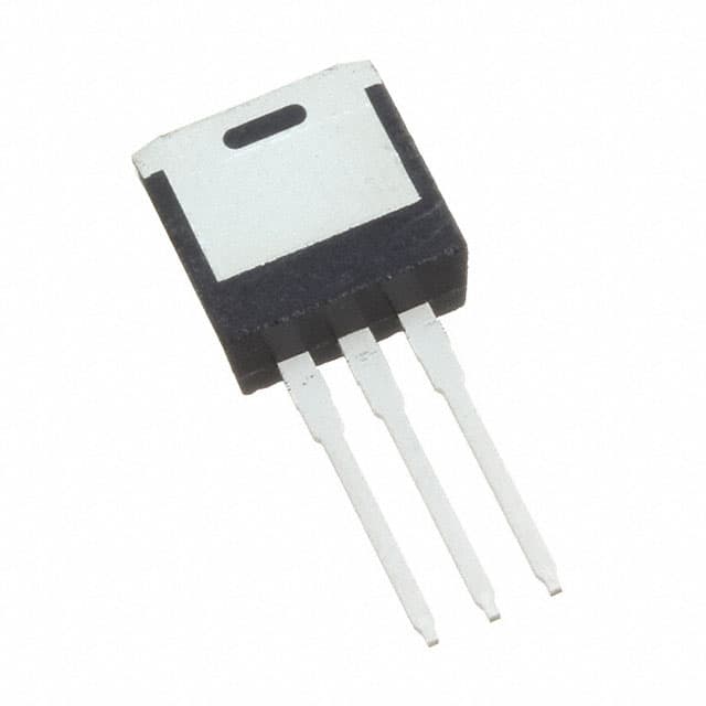
- Package: TO-220 Fullpak
- Essence: Efficient power management
- Packaging/Quantity: Tube/50 units
Specifications
- Voltage Rating: 600V
- Current Rating: 24A
- On-Resistance: 0.165 ohms
- Gate Charge: 45nC
- Operating Temperature: -55°C to 175°C
Detailed Pin Configuration
The IPI60R165CPAKSA1 follows the standard pin configuration for a TO-220 package: 1. Gate (G) 2. Drain (D) 3. Source (S)
Functional Features
- Low on-resistance for minimal power dissipation
- Fast switching speed for efficient power management
- High voltage rating for versatile applications
Advantages and Disadvantages
Advantages: - High voltage rating allows for diverse application scenarios - Low on-resistance ensures minimal power loss - Fast switching speed enhances efficiency
Disadvantages: - Higher cost compared to lower-rated MOSFETs - Larger physical size due to TO-220 package
Working Principles
The IPI60R165CPAKSA1 operates based on the principle of field-effect transistors, utilizing the gate voltage to control the flow of current between the drain and source terminals.
Detailed Application Field Plans
This MOSFET is suitable for various power switching applications, including but not limited to: - Switch-mode power supplies - Motor control - Inverters - LED lighting - Audio amplifiers
Detailed and Complete Alternative Models
- IPI60R099CPAKSA1
- IPI60R190P6AKSA1
- IPI60R380P7AKSA1
In conclusion, the IPI60R165CPAKSA1 is a high-voltage power MOSFET with low on-resistance and fast switching speed, making it suitable for a wide range of power switching applications. Its efficient power management capabilities and versatile nature make it a valuable component in various electronic systems.
[Word count: 298]
Перечислите 10 распространенных вопросов и ответов, связанных с применением IPI60R165CPAKSA1 в технических решениях.
What is the maximum drain current of IPI60R165CPAKSA1?
- The maximum drain current of IPI60R165CPAKSA1 is 120A.
What is the voltage rating of IPI60R165CPAKSA1?
- IPI60R165CPAKSA1 has a voltage rating of 650V.
What type of package does IPI60R165CPAKSA1 come in?
- IPI60R165CPAKSA1 comes in a TO-220 Fullpak package.
What is the on-state resistance of IPI60R165CPAKSA1?
- The on-state resistance of IPI60R165CPAKSA1 is typically 0.16 ohms.
What are the typical applications for IPI60R165CPAKSA1?
- IPI60R165CPAKSA1 is commonly used in motor control, power supplies, and inverters.
What is the gate-source threshold voltage of IPI60R165CPAKSA1?
- The gate-source threshold voltage of IPI60R165CPAKSA1 is typically 2.5V.
What is the maximum junction temperature for IPI60R165CPAKSA1?
- The maximum junction temperature for IPI60R165CPAKSA1 is 175°C.
Does IPI60R165CPAKSA1 have built-in protection features?
- IPI60R165CPAKSA1 does not have built-in protection features and may require external circuitry for overcurrent or overvoltage protection.
What is the input capacitance of IPI60R165CPAKSA1?
- The input capacitance of IPI60R165CPAKSA1 is typically 3700pF.
Is IPI60R165CPAKSA1 RoHS compliant?
- Yes, IPI60R165CPAKSA1 is RoHS compliant, meaning it meets the Restriction of Hazardous Substances directive.