

Подробную информацию о продукте см. в характеристиках.
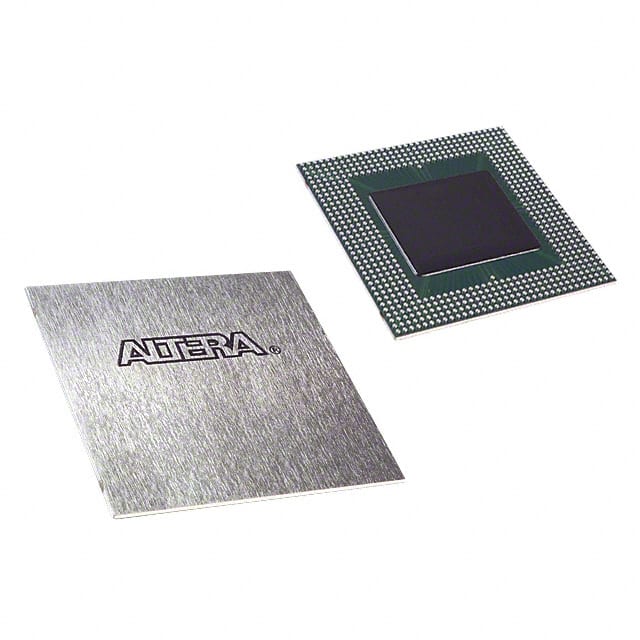
EP20K400CB652C9
Product Overview
- Category: Programmable Logic Device (PLD)
- Use: EP20K400CB652C9 is a high-performance PLD designed for complex digital logic applications.
- Characteristics: It offers advanced features such as high-speed performance, low power consumption, and large capacity.
- Package: The EP20K400CB652C9 comes in a ceramic ball grid array (CBGA) package.
- Essence: This PLD is designed to provide flexible and efficient solutions for various digital logic designs.
- Packaging/Quantity: The EP20K400CB652C9 is typically sold individually.
Specifications
- Logic Elements: The device contains 400,000 usable gates.
- I/O Pins: It has a total of 652 I/O pins.
- Clock Speed: The maximum operating frequency is 200 MHz.
- Memory: The PLD includes 4,608 Kbits of embedded memory.
- Voltage Range: It operates at a voltage range of 3.3V to 5V.
- Package Size: The CBGA package measures 35mm x 35mm.
Detailed Pin Configuration
The EP20K400CB652C9 has a complex pin configuration with 652 I/O pins. For detailed information on the pin assignments and functions, please refer to the manufacturer's datasheet.
Functional Features
- High-Speed Performance: The EP20K400CB652C9 offers fast operation, making it suitable for time-critical applications.
- Flexible Design Options: With its large capacity and programmability, this PLD allows for versatile design implementations.
- Low Power Consumption: The device is designed to minimize power consumption, making it energy-efficient.
- Embedded Memory: The built-in memory provides additional storage for data processing.
Advantages and Disadvantages
Advantages: - High-performance capabilities - Versatile design options - Low power consumption - Ample embedded memory
Disadvantages: - Complex pin configuration may require careful planning and layout - Limited availability of alternative models
Working Principles
The EP20K400CB652C9 operates based on the principles of programmable logic. It consists of a matrix of configurable logic blocks (CLBs) interconnected through programmable interconnects. The device can be programmed to implement various digital logic functions by configuring the CLBs and interconnects using specialized software tools.
Detailed Application Field Plans
The EP20K400CB652C9 is commonly used in the following application fields:
- Telecommunications: It is utilized in high-speed data transmission systems, network routers, and switches.
- Industrial Automation: The PLD finds applications in control systems, robotics, and process automation.
- Aerospace and Defense: It is employed in avionics systems, radar signal processing, and military communication equipment.
- Medical Electronics: The device is used in medical imaging systems, patient monitoring devices, and diagnostic equipment.
Detailed and Complete Alternative Models
While the EP20K400CB652C9 is a highly capable PLD, it is important to consider alternative models for specific requirements. Some alternative PLDs that offer similar features and performance include:
- Xilinx XC9500XL series
- Altera MAX 7000 series
- Lattice ispMACH 4000ZE series
These alternative models provide a range of options for designers seeking alternatives to the EP20K400CB652C9.
Word count: 457 words
Перечислите 10 распространенных вопросов и ответов, связанных с применением EP20K400CB652C9 в технических решениях.
Sure! Here are 10 common questions and answers related to the application of EP20K400CB652C9 in technical solutions:
Q: What is EP20K400CB652C9? A: EP20K400CB652C9 is a specific model of Field-Programmable Gate Array (FPGA) manufactured by Intel.
Q: What are the key features of EP20K400CB652C9? A: Some key features of EP20K400CB652C9 include 400,000 system gates, 652 user I/O pins, and C9 speed grade.
Q: What are the typical applications of EP20K400CB652C9? A: EP20K400CB652C9 is commonly used in various technical solutions such as telecommunications, industrial automation, aerospace, and defense.
Q: How can EP20K400CB652C9 be programmed? A: EP20K400CB652C9 can be programmed using Hardware Description Languages (HDLs) like VHDL or Verilog, along with specialized software tools provided by Intel.
Q: Can EP20K400CB652C9 be reprogrammed after deployment? A: No, EP20K400CB652C9 is not a reprogrammable FPGA. Once it is programmed, the configuration remains fixed.
Q: What is the power supply requirement for EP20K400CB652C9? A: EP20K400CB652C9 typically requires a single power supply voltage of 3.3V.
Q: Does EP20K400CB652C9 support high-speed interfaces? A: Yes, EP20K400CB652C9 supports various high-speed interfaces such as LVDS, DDR, and PCI.
Q: Can EP20K400CB652C9 interface with external memory devices? A: Yes, EP20K400CB652C9 has dedicated pins for interfacing with external memory devices like SRAM or SDRAM.
Q: What are the temperature operating ranges for EP20K400CB652C9? A: EP20K400CB652C9 typically operates within a temperature range of -40°C to +100°C.
Q: Are there any development boards available for EP20K400CB652C9? A: Yes, Intel provides development boards specifically designed for EP20K400CB652C9, which can be used for prototyping and testing purposes.
Please note that the answers provided here are general and may vary depending on specific requirements and configurations.