

Подробную информацию о продукте см. в характеристиках.
LC4128C-75TN128I
Product Overview
Category
LC4128C-75TN128I belongs to the category of programmable logic devices (PLDs).
Use
This product is commonly used in digital circuit design and implementation. It provides a flexible and customizable solution for various applications.
Characteristics
- Programmable: LC4128C-75TN128I can be programmed to perform specific functions according to the user's requirements.
- High-density: This PLD offers a high number of logic elements, allowing for complex designs.
- Low power consumption: LC4128C-75TN128I is designed to operate efficiently with minimal power consumption.
- Fast operation: The device offers high-speed performance, enabling quick execution of logic operations.
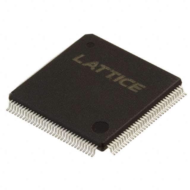
Package
LC4128C-75TN128I comes in a compact package that ensures easy integration into electronic circuits.
Essence
The essence of LC4128C-75TN128I lies in its ability to provide reconfigurable logic functionality, allowing designers to implement custom logic solutions without the need for dedicated hardware.
Packaging/Quantity
This product is typically packaged in trays or reels, with each containing a specific quantity of LC4128C-75TN128I devices.
Specifications
- Model: LC4128C-75TN128I
- Logic Elements: 1280
- I/O Pins: 75
- Operating Voltage: 3.3V
- Speed Grade: -75
- Package Type: TN128
Detailed Pin Configuration
The pin configuration of LC4128C-75TN128I is as follows:
- VCCIO
- GND
- IO0
- IO1
- IO2
- IO3
- IO4
- IO5
- IO6
- IO7
- IO8
- IO9
- IO10
- IO11
- IO12
- IO13
- IO14
- IO15
- IO16
- IO17
- IO18
- IO19
- IO20
- IO21
- IO22
- IO23
- IO24
- IO25
- IO26
- IO27
- IO28
- IO29
- IO30
- IO31
- IO32
- IO33
- IO34
- IO35
- IO36
- IO37
- IO38
- IO39
- IO40
- IO41
- IO42
- IO43
- IO44
- IO45
- IO46
- IO47
- IO48
- IO49
- IO50
- IO51
- IO52
- IO53
- IO54
- IO55
- IO56
- IO57
- IO58
- IO59
- IO60
- IO61
- IO62
- IO63
- IO64
- IO65
- IO66
- IO67
- IO68
- IO69
- IO70
- IO71
- IO72
- IO73
- IO74
- IO75
- GND
- VCCIO
Functional Features
- Reconfigurable Logic: LC4128C-75TN128I allows users to modify the logic functions it performs, providing flexibility in circuit design.
- High-Speed Operation: The device offers fast operation, enabling efficient execution of complex logic operations.
- Low Power Consumption: LC4128C-75TN128I is designed to minimize power consumption, making it suitable for battery-powered applications.
- I/O Flexibility: With 75 I/O pins, this PLD provides ample connectivity options for interfacing with other components.
Advantages and Disadvantages
Advantages
- Flexibility in circuit design
- High-speed operation
- Low power consumption
- Ample I/O options
Disadvantages
- Limited logic elements compared to higher-density PLDs
- Requires programming expertise for optimal utilization
Working Principles
LC4128C-75TN128I operates based on the principles of reconfigurable logic. It consists of a matrix of programmable logic elements interconnected through configurable routing resources. These logic elements can be programmed to perform specific functions, allowing designers to create custom logic circuits.
The device utilizes a combination of look-up tables (LUTs), flip-flops, and interconnect resources to implement desired logic functionality. By configuring the interconnections between
Перечислите 10 распространенных вопросов и ответов, связанных с применением LC4128C-75TN128I в технических решениях.
Sure! Here are 10 common questions and answers related to the application of LC4128C-75TN128I in technical solutions:
Q: What is LC4128C-75TN128I? A: LC4128C-75TN128I is a specific model of programmable logic device (PLD) manufactured by Lattice Semiconductor.
Q: What are the key features of LC4128C-75TN128I? A: LC4128C-75TN128I offers 128 macrocells, 75MHz maximum operating frequency, and 3.3V power supply compatibility.
Q: In what types of technical solutions can LC4128C-75TN128I be used? A: LC4128C-75TN128I can be used in various applications such as industrial control systems, automotive electronics, telecommunications, and consumer electronics.
Q: How does LC4128C-75TN128I differ from other PLDs? A: LC4128C-75TN128I stands out due to its low power consumption, small form factor, and high reliability.
Q: Can LC4128C-75TN128I be reprogrammed after deployment? A: Yes, LC4128C-75TN128I is a programmable device that can be reconfigured multiple times even after it has been deployed in a system.
Q: What programming languages or tools are compatible with LC4128C-75TN128I? A: LC4128C-75TN128I can be programmed using popular hardware description languages (HDLs) such as VHDL or Verilog, and it is supported by various development tools provided by Lattice Semiconductor.
Q: Are there any limitations to the number of inputs and outputs in LC4128C-75TN128I? A: LC4128C-75TN128I supports up to 128 inputs and outputs, providing flexibility for a wide range of applications.
Q: Can LC4128C-75TN128I interface with other components or devices? A: Yes, LC4128C-75TN128I can interface with other digital components or devices through standard protocols such as I2C, SPI, UART, or GPIO.
Q: What is the typical power consumption of LC4128C-75TN128I? A: The power consumption of LC4128C-75TN128I depends on the specific design and usage scenario, but it is generally known for its low power characteristics.
Q: Where can I find more information about using LC4128C-75TN128I in technical solutions? A: You can refer to the datasheet, application notes, and technical documentation provided by Lattice Semiconductor. Additionally, online forums and communities dedicated to programmable logic devices can be helpful resources for further information and support.