

Подробную информацию о продукте см. в характеристиках.
LC5512MV-75FN484C
Product Overview
Category: Integrated Circuit (IC)
Use: The LC5512MV-75FN484C is a high-performance programmable logic device designed for various digital applications. It offers advanced functionality and flexibility, making it suitable for a wide range of electronic systems.
Characteristics: - High-speed operation - Low power consumption - Large capacity - Flexible programming options - Robust design for reliable performance
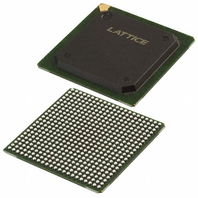
Package: The LC5512MV-75FN484C is available in a 484-pin Fine-Pitch Ball Grid Array (FBGA) package. This compact package ensures efficient use of board space and facilitates easy integration into electronic circuits.
Essence: The essence of the LC5512MV-75FN484C lies in its ability to provide customizable logic functions, enabling designers to implement complex digital systems with ease. Its versatile features make it an essential component in modern electronic devices.
Packaging/Quantity: The LC5512MV-75FN484C is typically supplied in reels or trays, depending on the manufacturer's packaging standards. The exact quantity per package may vary, but it is commonly available in quantities suitable for both prototyping and mass production.
Specifications
- Logic Cells: 5,512
- Operating Voltage: 3.3V
- Speed Grade: 75MHz
- I/O Pins: 484
- Programmable Gates: Yes
- Memory Blocks: Yes
- Clock Management: Yes
- Package Type: FBGA
- Temperature Range: -40°C to +85°C
Detailed Pin Configuration
The LC5512MV-75FN484C has a total of 484 pins, each serving a specific function within the integrated circuit. A detailed pin configuration diagram can be found in the product datasheet provided by the manufacturer.
Functional Features
- High-speed operation: The LC5512MV-75FN484C offers fast signal processing capabilities, making it suitable for applications that require real-time data handling.
- Flexible programming options: The device can be programmed to implement various logic functions, allowing designers to customize its behavior according to specific application requirements.
- Large capacity: With 5,512 logic cells and memory blocks, the LC5512MV-75FN484C provides ample resources for implementing complex digital systems.
- Clock management: The integrated clock management circuitry ensures precise timing control, enabling synchronous operation with other components in the system.
Advantages and Disadvantages
Advantages: - Versatile functionality - High-performance operation - Low power consumption - Compact package size - Reliable and robust design
Disadvantages: - Limited availability of alternative models - Higher cost compared to some lower-end programmable logic devices
Working Principles
The LC5512MV-75FN484C operates based on the principles of programmable logic. It consists of a network of configurable logic cells interconnected through programmable routing resources. These logic cells can be programmed to perform various logical operations, such as AND, OR, and XOR, allowing the device to implement complex digital functions.
The configuration of the LC5512MV-75FN484C is stored in non-volatile memory, ensuring that the programmed logic remains intact even after power is removed. This feature allows for easy reconfiguration and flexibility in adapting the device to different application requirements.
Detailed Application Field Plans
The LC5512MV-75FN484C finds applications in a wide range of fields, including but not limited to: - Telecommunications - Industrial automation - Consumer electronics - Automotive systems - Medical devices - Aerospace and defense
Its versatility and high-performance characteristics make it suitable for applications that require advanced digital processing capabilities.
Detailed and Complete Alternative Models
While the LC5512MV-75FN484C offers a unique combination of features, there are alternative models available in the market that cater to similar requirements. Some notable alternatives include: - Xilinx Spartan-6 FPGA series - Altera Cyclone IV FPGA series - Lattice ECP5 FPGA series
These alternative models provide comparable functionality and performance, allowing designers to choose the most suitable option based on their specific needs.
In conclusion, the LC5512MV-75FN484C is a high-performance programmable logic device with versatile functionality and flexible programming options. Its compact package, low power consumption, and reliable design make it an ideal choice for various digital applications across different industries.
Перечислите 10 распространенных вопросов и ответов, связанных с применением LC5512MV-75FN484C в технических решениях.
Sure! Here are 10 common questions and answers related to the application of LC5512MV-75FN484C in technical solutions:
1. What is LC5512MV-75FN484C? - LC5512MV-75FN484C is a specific model of Field-Programmable Gate Array (FPGA) manufactured by Lattice Semiconductor.
2. What are the key features of LC5512MV-75FN484C? - Some key features of LC5512MV-75FN484C include 5120 Look-Up Tables (LUTs), 120 Input/Output (I/O) pins, 75 MHz maximum operating frequency, and 484-pin Fine-Pitch Ball Grid Array (FBGA) package.
3. What are the typical applications of LC5512MV-75FN484C? - LC5512MV-75FN484C can be used in various applications such as industrial automation, telecommunications, automotive electronics, medical devices, and consumer electronics.
4. How can LC5512MV-75FN484C be programmed? - LC5512MV-75FN484C can be programmed using Hardware Description Languages (HDL) like VHDL or Verilog, which allow users to describe the desired functionality of the FPGA.
5. Can LC5512MV-75FN484C be reprogrammed after initial programming? - Yes, LC5512MV-75FN484C is a reprogrammable FPGA, which means it can be reconfigured multiple times with different designs.
6. What development tools are available for working with LC5512MV-75FN484C? - Lattice Semiconductor provides software tools like Lattice Diamond or Lattice Radiant, which offer design entry, synthesis, simulation, and programming capabilities for working with LC5512MV-75FN484C.
7. What is the power supply requirement for LC5512MV-75FN484C? - The typical power supply voltage for LC5512MV-75FN484C is 3.3V, but it also supports a wide range of voltages from 2.375V to 3.465V.
8. Can LC5512MV-75FN484C interface with other components or devices? - Yes, LC5512MV-75FN484C has multiple I/O pins that can be used to interface with other components or devices such as sensors, memory modules, communication interfaces, and more.
9. Is there any documentation available for LC5512MV-75FN484C? - Yes, Lattice Semiconductor provides datasheets, user guides, application notes, and reference designs for LC5512MV-75FN484C on their official website.
10. Are there any limitations or considerations when using LC5512MV-75FN484C? - Some considerations include understanding the FPGA's timing constraints, power consumption, and ensuring proper cooling for reliable operation. Additionally, it's important to have a good understanding of the specific requirements of your application to ensure the FPGA meets your needs.
Please note that these answers are general and may vary depending on the specific requirements and use cases of LC5512MV-75FN484C in different technical solutions.