

Подробную информацию о продукте см. в характеристиках.
LCMXO2-7000HC-5BG332C
Product Overview
Category
The LCMXO2-7000HC-5BG332C belongs to the category of Field Programmable Gate Arrays (FPGAs).
Use
FPGAs are integrated circuits that can be programmed after manufacturing. The LCMXO2-7000HC-5BG332C is specifically designed for digital logic applications.
Characteristics
- Low power consumption
- High performance
- Small form factor
- Flexible and reconfigurable
Package
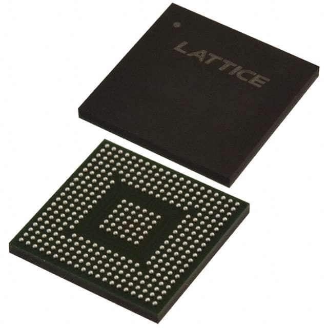
The LCMXO2-7000HC-5BG332C comes in a BGA (Ball Grid Array) package.
Essence
The essence of the LCMXO2-7000HC-5BG332C lies in its ability to provide a customizable hardware solution for various digital logic applications.
Packaging/Quantity
The LCMXO2-7000HC-5BG332C is typically packaged individually and is available in various quantities depending on the manufacturer.
Specifications
- Model: LCMXO2-7000HC-5BG332C
- Logic Elements: 7,000
- Speed Grade: -5
- Package Type: BGA
- Package Pins: 332
- Operating Voltage: 3.3V
- Maximum Frequency: 100 MHz
- I/O Standards: LVCMOS, LVTTL, SSTL, HSTL
Detailed Pin Configuration
The LCMXO2-7000HC-5BG332C has a total of 332 pins. These pins are used for various purposes such as input/output connections, clock signals, power supply, and configuration.
For a detailed pin configuration diagram, please refer to the datasheet provided by the manufacturer.
Functional Features
- Reconfigurable logic elements
- Embedded memory blocks
- Dedicated digital signal processing (DSP) blocks
- Built-in clock management resources
- Support for various I/O standards
Advantages and Disadvantages
Advantages
- Flexibility in design and customization
- Low power consumption
- High performance
- Small form factor
- Cost-effective compared to custom ASICs
Disadvantages
- Limited number of logic elements compared to larger FPGAs
- Higher cost compared to microcontrollers for simple applications
- Steeper learning curve for programming and utilization
Working Principles
The LCMXO2-7000HC-5BG332C works based on the principles of reconfigurable hardware. It consists of a matrix of configurable logic elements that can be programmed to perform specific functions. The configuration data is stored in non-volatile memory and can be modified as needed.
When powered on, the FPGA loads the configuration data and establishes the desired circuit connections. This allows the user to create custom digital logic circuits without the need for dedicated hardware.
Detailed Application Field Plans
The LCMXO2-7000HC-5BG332C finds applications in various fields, including:
- Communications: Used in wireless base stations, network routers, and communication protocols.
- Industrial Automation: Employed in control systems, robotics, and process automation.
- Automotive: Utilized in vehicle electronics, driver assistance systems, and infotainment systems.
- Aerospace: Integrated into avionics, satellite communication systems, and flight control systems.
- Consumer Electronics: Found in smart devices, gaming consoles, and multimedia systems.
Detailed and Complete Alternative Models
- LCMXO2-1200HC-4TG100C
- LCMXO2-2000HC-4TG144C
- LCMXO2-4000HC-4TG144C
- LCMXO2-7000HC-4BG400C
These alternative models offer varying logic element counts, package types, and pin configurations to cater to different project requirements.
In conclusion, the LCMXO2-7000HC-5BG332C is a versatile FPGA that provides a customizable hardware solution for digital logic applications. Its low power consumption, high performance, and flexibility make it suitable for a wide range of industries.
Перечислите 10 распространенных вопросов и ответов, связанных с применением LCMXO2-7000HC-5BG332C в технических решениях.
Sure! Here are 10 common questions and answers related to the application of LCMXO2-7000HC-5BG332C in technical solutions:
Q: What is the LCMXO2-7000HC-5BG332C? A: The LCMXO2-7000HC-5BG332C is a low-cost, low-power FPGA (Field-Programmable Gate Array) device manufactured by Lattice Semiconductor.
Q: What are the key features of LCMXO2-7000HC-5BG332C? A: Some key features include 7000 Look-Up Tables (LUTs), 332 user I/O pins, low power consumption, and support for various I/O standards.
Q: What are some typical applications of LCMXO2-7000HC-5BG332C? A: It can be used in a wide range of applications such as industrial automation, consumer electronics, communication systems, and embedded control systems.
Q: How can I program the LCMXO2-7000HC-5BG332C? A: You can program the device using Lattice Diamond or iCEcube2 software tools provided by Lattice Semiconductor.
Q: What programming languages are supported by LCMXO2-7000HC-5BG332C? A: The device supports VHDL and Verilog hardware description languages for programming.
Q: Can I use LCMXO2-7000HC-5BG332C for real-time signal processing? A: Yes, the device's high-speed I/O pins and programmable logic make it suitable for real-time signal processing applications.
Q: Does LCMXO2-7000HC-5BG332C support communication protocols like UART, SPI, and I2C? A: Yes, the device supports various communication protocols through its user I/O pins.
Q: What is the power consumption of LCMXO2-7000HC-5BG332C? A: The device has low power consumption, typically ranging from a few milliwatts to a few watts depending on the application.
Q: Can I use LCMXO2-7000HC-5BG332C for high-speed data processing? A: While the device is capable of handling high-speed data, it is important to consider the specific requirements of your application and design accordingly.
Q: Are there any development boards or evaluation kits available for LCMXO2-7000HC-5BG332C? A: Yes, Lattice Semiconductor offers development boards and evaluation kits specifically designed for LCMXO2-7000HC-5BG332C, which can help in prototyping and testing your designs.
Please note that these answers are general and may vary based on specific requirements and application scenarios.