

Подробную информацию о продукте см. в характеристиках.
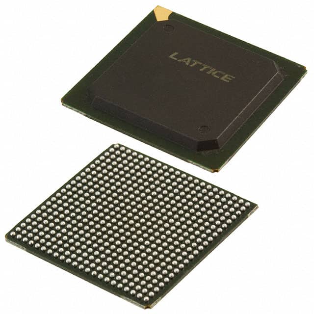
LCMXO2-7000HE-6FG484I
Product Overview
Category
The LCMXO2-7000HE-6FG484I belongs to the category of Field-Programmable Gate Arrays (FPGAs).
Use
FPGAs are integrated circuits that can be programmed and reprogrammed to perform various digital functions. The LCMXO2-7000HE-6FG484I is specifically designed for applications requiring low power consumption and high performance.
Characteristics
- Low power consumption: The LCMXO2-7000HE-6FG484I is optimized for low power operation, making it suitable for battery-powered devices.
- High performance: It offers a high logic density and fast performance, enabling complex digital designs to be implemented efficiently.
- Small package size: The FPGA is housed in a 484-pin Fine-Pitch Ball Grid Array (FBGA) package, which allows for compact designs.
- Enhanced security features: The LCMXO2-7000HE-6FG484I includes security features such as bitstream encryption and tamper detection, ensuring the integrity of the design.
Package and Quantity
The LCMXO2-7000HE-6FG484I is available in a 484-pin FBGA package. The quantity may vary depending on the supplier or manufacturer.
Specifications
- Logic Elements: 7,000
- Look-Up Tables (LUTs): 4,500
- Flip-Flops: 9,600
- Block RAM: 270 Kbits
- Maximum User I/Os: 266
- Operating Voltage: 1.2V
- Speed Grade: -6 (indicates the maximum operating frequency)
Detailed Pin Configuration
The LCMXO2-7000HE-6FG484I has a total of 484 pins. These pins are used for various purposes, including input/output connections, power supply, configuration, and programming. A detailed pin configuration diagram can be found in the product datasheet.
Functional Features
- Programmability: The LCMXO2-7000HE-6FG484I can be programmed using Hardware Description Languages (HDLs) such as VHDL or Verilog, allowing for flexible and customizable digital designs.
- Reconfigurability: FPGAs can be reprogrammed multiple times, making them suitable for prototyping, testing, and iterative design processes.
- Integration: The FPGA integrates various components such as Look-Up Tables, Flip-Flops, and Block RAM, enabling the implementation of complex digital systems on a single chip.
- I/O Flexibility: The LCMXO2-7000HE-6FG484I provides a range of user I/Os, allowing for easy interfacing with external devices and peripherals.
Advantages and Disadvantages
Advantages
- Low power consumption enables energy-efficient designs.
- High logic density allows for complex designs to be implemented efficiently.
- Reconfigurability offers flexibility during the design and development process.
- Enhanced security features protect the integrity of the design.
Disadvantages
- Limited resources compared to larger FPGAs, which may restrict the complexity of designs that can be implemented.
- Higher cost compared to other programmable logic devices, such as microcontrollers or Application-Specific Integrated Circuits (ASICs).
Working Principles
FPGAs consist of an array of configurable logic blocks interconnected through programmable routing resources. The LCMXO2-7000HE-6FG484I utilizes Look-Up Tables (LUTs) and Flip-Flops to implement digital functions. The behavior of the FPGA is defined by the configuration data stored in its memory cells. During operation, the FPGA executes the programmed logic based on the input signals, producing the desired output.
Detailed Application Field Plans
The LCMXO2-7000HE-6FG484I is suitable for a wide range of applications, including but not limited to: - Embedded systems - Industrial automation - Communications equipment - Consumer electronics - Medical devices - Automotive electronics
Its low power consumption, high performance, and reconfigurability make it an ideal choice for these application fields.
Detailed and Complete Alternative Models
Some alternative models to the LCMXO2-7000HE-6FG484I include: - LCMXO2-1200ZE-1TG144C - LCMXO3LF-6900C-5BG256C - LCMXO3L-4300E-5MG324C
These models offer different specifications and features, providing options for various design requirements.
Word count: 550 words
Перечислите 10 распространенных вопросов и ответов, связанных с применением LCMXO2-7000HE-6FG484I в технических решениях.
Sure! Here are 10 common questions and answers related to the application of LCMXO2-7000HE-6FG484I in technical solutions:
Q: What is the LCMXO2-7000HE-6FG484I? A: The LCMXO2-7000HE-6FG484I is a low-cost, low-power FPGA (Field-Programmable Gate Array) device manufactured by Lattice Semiconductor.
Q: What are the key features of the LCMXO2-7000HE-6FG484I? A: Some key features include 7000 Look-Up Tables (LUTs), 128 Kbits of embedded block RAM, 34 I/O pins, and support for various I/O standards.
Q: What are some typical applications of the LCMXO2-7000HE-6FG484I? A: The LCMXO2-7000HE-6FG484I is commonly used in applications such as industrial control systems, consumer electronics, medical devices, and communication equipment.
Q: How can I program the LCMXO2-7000HE-6FG484I? A: The LCMXO2-7000HE-6FG484I can be programmed using Lattice Diamond or Lattice Radiant software tools, which provide a graphical interface for designing and programming the FPGA.
Q: What power supply voltage does the LCMXO2-7000HE-6FG484I require? A: The LCMXO2-7000HE-6FG484I operates at a nominal core voltage of 1.2V and requires an external power supply within the range of 1.14V to 1.26V.
Q: Can I use the LCMXO2-7000HE-6FG484I in battery-powered applications? A: Yes, the LCMXO2-7000HE-6FG484I is designed to be power-efficient and can be used in battery-powered applications where low power consumption is crucial.
Q: Does the LCMXO2-7000HE-6FG484I support any communication protocols? A: Yes, the LCMXO2-7000HE-6FG484I supports various communication protocols such as SPI (Serial Peripheral Interface), I2C (Inter-Integrated Circuit), and UART (Universal Asynchronous Receiver-Transmitter).
Q: Can I interface the LCMXO2-7000HE-6FG484I with external memory devices? A: Yes, the LCMXO2-7000HE-6FG484I has embedded block RAM and can also interface with external memory devices using its I/O pins.
Q: What are the temperature specifications for the LCMXO2-7000HE-6FG484I? A: The LCMXO2-7000HE-6FG484I has an operating temperature range of -40°C to 85°C.
Q: Are there any development boards available for the LCMXO2-7000HE-6FG484I? A: Yes, Lattice Semiconductor offers development boards like the iCEstick Evaluation Kit that are compatible with the LCMXO2-7000HE-6FG484I and provide a platform for prototyping and testing.