

Подробную информацию о продукте см. в характеристиках.
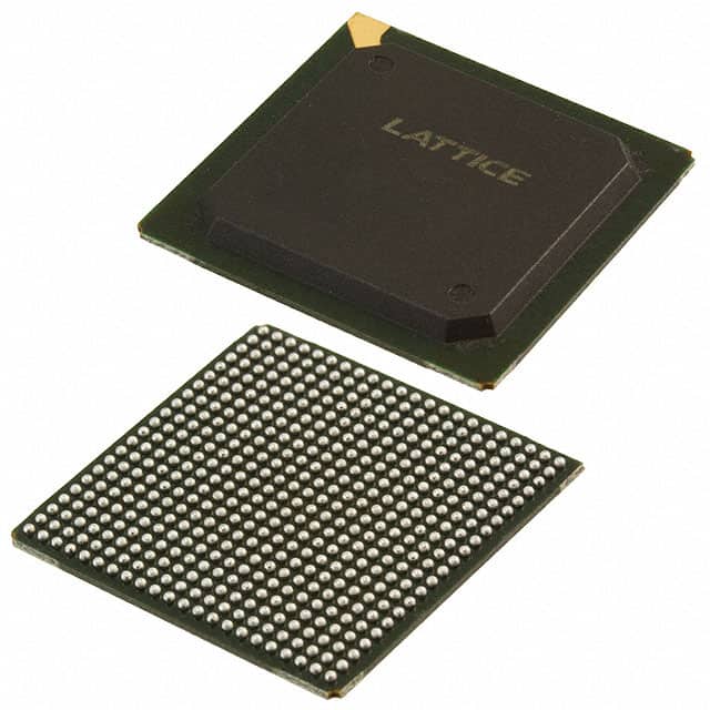
LCMXO2-7000ZE-1FG484C
Product Overview
Category
The LCMXO2-7000ZE-1FG484C belongs to the category of Field-Programmable Gate Arrays (FPGAs).
Use
FPGAs are integrated circuits that can be programmed after manufacturing, allowing for flexible and customizable digital logic designs. The LCMXO2-7000ZE-1FG484C is specifically designed for applications requiring low power consumption and small form factor.
Characteristics
- Low power consumption
- Small form factor
- High performance
- Programmable logic cells
- Embedded memory blocks
- Flexible I/O options
Package
The LCMXO2-7000ZE-1FG484C comes in a 484-pin Fine-Pitch Ball Grid Array (FBGA) package.
Essence
The essence of the LCMXO2-7000ZE-1FG484C lies in its ability to provide designers with a versatile and power-efficient solution for implementing custom digital logic designs.
Packaging/Quantity
The LCMXO2-7000ZE-1FG484C is typically sold individually or in reels, with each reel containing a specific quantity of units. The exact packaging and quantity may vary depending on the supplier.
Specifications
- Logic Cells: 7,000
- Look-Up Tables (LUTs): 4,500
- Flip-Flops: 9,000
- Block RAM: 270 Kbits
- Maximum User I/Os: 173
- Operating Voltage: 1.2V
- Speed Grade: -1
- Configuration Method: JTAG
Detailed Pin Configuration
The LCMXO2-7000ZE-1FG484C has a total of 484 pins, each serving a specific purpose in the FPGA's functionality. The pin configuration includes dedicated input/output pins, power supply pins, ground pins, and configuration pins. A detailed pinout diagram can be found in the product datasheet.
Functional Features
1. Low Power Consumption
The LCMXO2-7000ZE-1FG484C is designed to operate at low power levels, making it suitable for battery-powered applications or devices with strict power constraints.
2. Small Form Factor
With its compact package size and high integration capabilities, this FPGA is ideal for space-constrained designs where size optimization is crucial.
3. Programmable Logic Cells
The FPGA offers a large number of programmable logic cells, allowing designers to implement complex digital logic functions easily.
4. Embedded Memory Blocks
The LCMXO2-7000ZE-1FG484C includes embedded memory blocks, enabling efficient storage and retrieval of data within the FPGA itself.
5. Flexible I/O Options
The device provides a wide range of user I/O pins, supporting various communication protocols and interfacing requirements.
Advantages and Disadvantages
Advantages
- Low power consumption enables energy-efficient designs.
- Small form factor allows for compact and portable applications.
- High performance and flexibility due to programmable logic cells.
- Embedded memory blocks enhance data processing capabilities.
- Flexible I/O options enable seamless integration with external devices.
Disadvantages
- Limited logic capacity compared to larger FPGAs.
- Higher cost per logic cell compared to some alternatives.
- Complexity of programming and configuring the FPGA may require specialized knowledge.
Working Principles
The LCMXO2-7000ZE-1FG484C operates based on the principles of reconfigurable digital logic. It consists of an array of programmable logic cells interconnected through configurable routing resources. These logic cells can be programmed to implement desired digital functions by configuring the interconnections and functionality of the logic gates within each cell.
Detailed Application Field Plans
The LCMXO2-7000ZE-1FG484C finds applications in various fields, including:
- Embedded Systems: The FPGA can be used to implement custom hardware accelerators, interface controllers, or signal processing modules in embedded systems.
- Communications: It can be employed in communication systems for protocol conversion, data encryption/decryption, or signal modulation/demodulation.
- Industrial Automation: The FPGA can enable real-time control and monitoring of industrial processes, such as motor control, machine vision, or sensor interfacing.
- Medical Devices: It can be utilized in medical equipment for image processing, patient monitoring, or diagnostic systems.
- Internet of Things (IoT): The FPGA can be integrated into IoT devices for edge computing, sensor fusion, or secure communication.
Detailed and Complete Alternative Models
- Xilinx Spartan-6 XC6SLX9
- Altera Cyclone IV EP4CE6
- Microsemi IGLOO2
Перечислите 10 распространенных вопросов и ответов, связанных с применением LCMXO2-7000ZE-1FG484C в технических решениях.
Sure! Here are 10 common questions and answers related to the application of LCMXO2-7000ZE-1FG484C in technical solutions:
Q1: What is the LCMXO2-7000ZE-1FG484C? A1: The LCMXO2-7000ZE-1FG484C is a low-cost, low-power FPGA (Field-Programmable Gate Array) device manufactured by Lattice Semiconductor.
Q2: What are the key features of LCMXO2-7000ZE-1FG484C? A2: Some key features of LCMXO2-7000ZE-1FG484C include 7000 Look-Up Tables (LUTs), 128 Kbits of embedded memory, 34 I/O pins, and support for various I/O standards.
Q3: What are the typical applications of LCMXO2-7000ZE-1FG484C? A3: LCMXO2-7000ZE-1FG484C is commonly used in applications such as industrial control systems, consumer electronics, communication devices, and automotive electronics.
Q4: How can I program the LCMXO2-7000ZE-1FG484C? A4: The LCMXO2-7000ZE-1FG484C can be programmed using Lattice Diamond or Lattice Radiant software tools, which provide a graphical interface for designing and programming the FPGA.
Q5: What voltage levels does LCMXO2-7000ZE-1FG484C support? A5: LCMXO2-7000ZE-1FG484C supports both 3.3V and 1.2V voltage levels, making it compatible with a wide range of digital logic circuits.
Q6: Can I use LCMXO2-7000ZE-1FG484C in battery-powered applications? A6: Yes, LCMXO2-7000ZE-1FG484C is designed to be low-power and can be used in battery-powered applications where power consumption is a concern.
Q7: Does LCMXO2-7000ZE-1FG484C support external memory interfaces? A7: Yes, LCMXO2-7000ZE-1FG484C supports various external memory interfaces such as SPI, I2C, and UART, allowing for easy integration with other devices.
Q8: Can I use LCMXO2-7000ZE-1FG484C for real-time signal processing? A8: Yes, LCMXO2-7000ZE-1FG484C's high-speed I/O pins and embedded memory make it suitable for real-time signal processing applications.
Q9: What development boards are available for LCMXO2-7000ZE-1FG484C? A9: Lattice Semiconductor offers several development boards, such as the iCE40 UltraPlus Breakout Board, which can be used for prototyping and evaluation of LCMXO2-7000ZE-1FG484C.
Q10: Are there any reference designs or application notes available for LCMXO2-7000ZE-1FG484C? A10: Yes, Lattice Semiconductor provides a wide range of reference designs and application notes on their website, which can help users get started with LCMXO2-7000ZE-1FG484C and implement various technical solutions.
Please note that the answers provided here are general and may vary depending on specific requirements and use cases. It is always recommended to refer to the official documentation and datasheets for accurate and up-to-date information.