

Подробную информацию о продукте см. в характеристиках.
LCMXO256E-3M100I
Product Overview
Category
The LCMXO256E-3M100I belongs to the category of Field-Programmable Gate Arrays (FPGAs).
Use
FPGAs are integrated circuits that can be programmed and reprogrammed to perform various digital functions. The LCMXO256E-3M100I is specifically designed for applications requiring high-performance and low-power consumption.
Characteristics
- High-performance FPGA with low power consumption
- Programmable and reprogrammable
- Suitable for a wide range of applications
- Compact package size
- Robust and reliable design
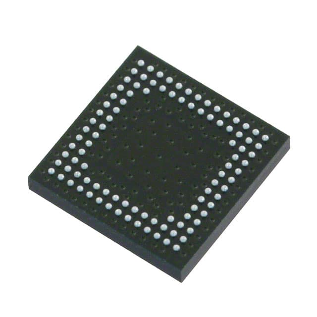
Package
The LCMXO256E-3M100I comes in a compact package, ensuring ease of integration into electronic systems. The package provides protection against environmental factors and facilitates efficient heat dissipation.
Essence
The essence of the LCMXO256E-3M100I lies in its ability to provide flexible and customizable digital functionality. It allows designers to implement complex logic circuits and algorithms without the need for custom hardware.
Packaging/Quantity
The LCMXO256E-3M100I is typically packaged individually and is available in various quantities depending on the requirements of the application.
Specifications
- FPGA Family: Lattice XO2
- Logic Cells: 256
- Maximum Operating Frequency: 100 MHz
- Programmable Logic Blocks: 256
- I/O Pins: 100
- Power Supply Voltage: 1.2V
- Operating Temperature Range: -40°C to 85°C
- Package Type: QFN
Detailed Pin Configuration
The LCMXO256E-3M100I has a total of 100 I/O pins, each serving a specific purpose in the system. The pin configuration includes input/output pins, power supply pins, and configuration pins. For a detailed pin configuration diagram, please refer to the product datasheet.
Functional Features
- High-performance FPGA architecture
- Low power consumption
- Flexible and customizable digital functionality
- Support for various communication protocols
- On-chip memory resources
- Built-in security features
- Easy integration with existing systems
Advantages and Disadvantages
Advantages
- Versatile and adaptable for a wide range of applications
- Cost-effective compared to custom hardware solutions
- Shorter development cycles due to programmability
- Lower power consumption compared to traditional ASICs
- Ability to reconfigure and update functionality as needed
Disadvantages
- Limited performance compared to dedicated ASICs for specific tasks
- Higher cost per unit compared to mass-produced standard components
- Steeper learning curve for programming and utilizing FPGA capabilities
Working Principles
The LCMXO256E-3M100I operates based on the principles of reconfigurable logic. It consists of an array of configurable logic blocks interconnected through programmable routing resources. The device can be programmed using Hardware Description Languages (HDL) such as VHDL or Verilog, allowing designers to define the desired functionality and interconnections between logic elements.
During operation, the FPGA executes the programmed logic by routing signals through the configured interconnections, enabling the implementation of complex digital circuits. The ability to reprogram the FPGA allows for iterative design improvements and updates without requiring physical hardware changes.
Detailed Application Field Plans
The LCMXO256E-3M100I finds application in various fields, including but not limited to:
- Communications: Used in wireless base stations, network routers, and data transmission equipment.
- Industrial Automation: Employed in control systems, robotics, and process automation.
- Automotive: Integrated into advanced driver-assistance systems (ADAS), infotainment systems, and engine control units.
- Aerospace: Utilized in avionics, satellite communication systems, and flight control systems.
- Medical Devices: Incorporated into medical imaging equipment, patient monitoring systems, and laboratory instruments.
Detailed and Complete Alternative Models
- LCMXO2-1200ZE-3MG132C
- LCMXO2-4000HE-4TG144C
- LCMXO3L-6900E-6BG484I
- LCMXO3LF-4300E-5BG256C
- LCMXO3LF-2100E-5BG256C
These alternative models offer similar functionality and performance characteristics to the LCMXO256E-3M100I, providing designers with a range of options to suit their specific requirements.
In conclusion, the LCMXO256E-3M100I is a high-performance FPGA that offers flexibility, low power consumption, and a compact package size. It finds applications in various industries and provides designers with the ability to implement complex digital circuits without the need for
Перечислите 10 распространенных вопросов и ответов, связанных с применением LCMXO256E-3M100I в технических решениях.
Sure! Here are 10 common questions and answers related to the application of LCMXO256E-3M100I in technical solutions:
Q: What is the LCMXO256E-3M100I? A: The LCMXO256E-3M100I is a low-cost, low-power FPGA (Field-Programmable Gate Array) device manufactured by Lattice Semiconductor.
Q: What are the key features of the LCMXO256E-3M100I? A: The key features include 256 LUTs (Look-Up Tables), 4Kbits of embedded memory, 32 I/O pins, and support for various I/O standards.
Q: What are some typical applications of the LCMXO256E-3M100I? A: The LCMXO256E-3M100I is commonly used in applications such as industrial automation, consumer electronics, communication systems, and IoT devices.
Q: How can I program the LCMXO256E-3M100I? A: The LCMXO256E-3M100I can be programmed using Lattice Diamond or Lattice Radiant software tools, which support various programming languages like VHDL and Verilog.
Q: Can the LCMXO256E-3M100I interface with other components or devices? A: Yes, the LCMXO256E-3M100I supports various I/O standards, allowing it to interface with other components or devices such as sensors, displays, and communication modules.
Q: What is the power consumption of the LCMXO256E-3M100I? A: The LCMXO256E-3M100I is designed to be low-power, with typical power consumption ranging from a few milliwatts to a few watts, depending on the application.
Q: Can I reprogram the LCMXO256E-3M100I multiple times? A: Yes, the LCMXO256E-3M100I is a reprogrammable FPGA, allowing you to modify and reconfigure its functionality multiple times as per your requirements.
Q: Are there any development boards available for the LCMXO256E-3M100I? A: Yes, Lattice Semiconductor provides development boards like the LCMXO256E-B-EVN, which can be used for prototyping and testing with the LCMXO256E-3M100I.
Q: What kind of support is available for the LCMXO256E-3M100I? A: Lattice Semiconductor offers technical documentation, application notes, reference designs, and online forums to provide support for the LCMXO256E-3M100I.
Q: Where can I purchase the LCMXO256E-3M100I? A: The LCMXO256E-3M100I can be purchased from authorized distributors or directly from Lattice Semiconductor's website.