

Подробную информацию о продукте см. в характеристиках.
LCMXO3LF-9400C-6BG484C
Product Overview
Category: Programmable Logic Device (PLD)
Use: The LCMXO3LF-9400C-6BG484C is a high-performance PLD designed for various digital logic applications. It offers flexibility and versatility in implementing complex digital circuits.
Characteristics: - Low power consumption - High-speed performance - Small form factor - Wide operating temperature range - Easy programmability
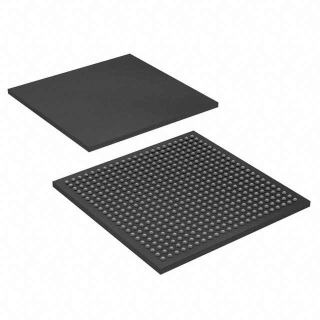
Package: The LCMXO3LF-9400C-6BG484C comes in a 484-ball FineLine BGA package, which provides excellent thermal dissipation and compact size.
Essence: This PLD is built to provide designers with a reliable and efficient solution for implementing digital logic circuits in a wide range of applications.
Packaging/Quantity: The LCMXO3LF-9400C-6BG484C is typically sold individually or in reels, depending on the manufacturer's packaging specifications.
Specifications
- Logic Elements: 9400
- Flip-Flops: 4700
- RAM Bits: 276480
- Maximum Operating Frequency: 300 MHz
- I/O Pins: 484
- Supply Voltage: 1.2V
- Operating Temperature Range: -40°C to 85°C
Detailed Pin Configuration
The LCMXO3LF-9400C-6BG484C has a total of 484 pins, each serving a specific purpose in the device's operation. A detailed pin configuration diagram can be found in the product datasheet provided by the manufacturer.
Functional Features
- High-speed performance allows for efficient execution of complex digital logic operations.
- Low power consumption ensures energy efficiency and longer battery life in portable devices.
- Flexible programmability enables customization and adaptation to various application requirements.
- Wide operating temperature range allows for reliable operation in harsh environments.
Advantages and Disadvantages
Advantages: - High-performance PLD suitable for a wide range of digital logic applications. - Low power consumption makes it ideal for battery-powered devices. - Small form factor enables integration into compact designs. - Easy programmability provides flexibility in circuit implementation.
Disadvantages: - Limited logic elements compared to higher-end PLDs. - May require additional support components for certain complex applications. - Higher cost compared to simpler programmable logic devices.
Working Principles
The LCMXO3LF-9400C-6BG484C operates based on the principles of programmable logic. It consists of configurable logic blocks (CLBs), interconnect resources, and I/O elements. The CLBs can be programmed to implement various digital logic functions, while the interconnect resources facilitate communication between different blocks. The I/O elements enable interaction with external devices.
Detailed Application Field Plans
The LCMXO3LF-9400C-6BG484C finds applications in a wide range of fields, including but not limited to: 1. Industrial automation 2. Consumer electronics 3. Automotive systems 4. Communication equipment 5. Medical devices
In industrial automation, this PLD can be used for control systems, motor drives, and sensor interfaces. In consumer electronics, it can be utilized for audio/video processing, gaming consoles, and smart home devices. Automotive systems can benefit from its use in engine control units, infotainment systems, and advanced driver-assistance systems. Communication equipment can incorporate this PLD for network switches, routers, and base stations. Medical devices can leverage its capabilities for patient monitoring, imaging systems, and laboratory equipment.
Detailed and Complete Alternative Models
- LCMXO2-1200ZE-1TG144C
- LCMXO2-4000HE-5TG144C
- LCMXO2-7000HE-4TG144C
- LCMXO2-1200HC-4TG144C
- LCMXO2-2000HC-4TG144C
These alternative models offer similar functionality and performance to the LCMXO3LF-9400C-6BG484C, but with varying logic element counts and I/O pin configurations. Designers can choose the most suitable model based on their specific requirements.
Note: The above information is subject to change. For the most accurate and up-to-date details, refer to the product datasheet provided by the manufacturer.
Word Count: 570
Перечислите 10 распространенных вопросов и ответов, связанных с применением LCMXO3LF-9400C-6BG484C в технических решениях.
Sure! Here are 10 common questions and answers related to the application of LCMXO3LF-9400C-6BG484C in technical solutions:
Q: What is the LCMXO3LF-9400C-6BG484C? A: The LCMXO3LF-9400C-6BG484C is a specific model of Field-Programmable Gate Array (FPGA) manufactured by Lattice Semiconductor.
Q: What is an FPGA? A: An FPGA is a type of integrated circuit that can be programmed or reconfigured after manufacturing, allowing for flexible hardware implementation of digital logic circuits.
Q: What are the key features of the LCMXO3LF-9400C-6BG484C? A: Some key features of this FPGA include 9400 LUTs (Look-Up Tables), 6 inputs per LUT, 484-ball grid array package, low power consumption, and support for various I/O standards.
Q: What are the typical applications of the LCMXO3LF-9400C-6BG484C? A: This FPGA is commonly used in applications such as industrial automation, automotive electronics, consumer electronics, communication systems, and medical devices.
Q: How can I program the LCMXO3LF-9400C-6BG484C? A: You can program this FPGA using the Lattice Diamond design software, which provides a graphical interface for designing and implementing your digital logic circuits.
Q: Can I use the LCMXO3LF-9400C-6BG484C for real-time signal processing? A: Yes, this FPGA is suitable for real-time signal processing tasks due to its high-speed performance and low-latency architecture.
Q: Does the LCMXO3LF-9400C-6BG484C support communication protocols like UART, SPI, or I2C? A: Yes, this FPGA supports various communication protocols, including UART, SPI, I2C, and others, through its configurable I/O pins.
Q: Can I interface the LCMXO3LF-9400C-6BG484C with external memory devices? A: Yes, this FPGA has dedicated pins for interfacing with external memory devices such as SRAM, SDRAM, and Flash memory.
Q: What is the power supply requirement for the LCMXO3LF-9400C-6BG484C? A: The recommended power supply voltage for this FPGA is typically 1.2V, but it can operate within a range of 1.14V to 1.26V.
Q: Are there any development boards available for prototyping with the LCMXO3LF-9400C-6BG484C? A: Yes, Lattice Semiconductor provides development boards like the LCMXO3L-EVN for prototyping and evaluation purposes with this FPGA.
Please note that the specific details and answers may vary depending on the manufacturer's documentation and specifications.