

Подробную информацию о продукте см. в характеристиках.
LT3753HFE#PBF
Product Overview
Category
The LT3753HFE#PBF belongs to the category of integrated circuits (ICs) specifically designed for power management applications.
Use
This IC is primarily used for controlling and regulating power in various electronic systems, such as power supplies, battery chargers, LED drivers, and other similar applications.
Characteristics
- High efficiency: The LT3753HFE#PBF offers high efficiency power conversion, minimizing energy losses.
- Wide input voltage range: It can handle a wide range of input voltages, making it suitable for diverse applications.
- Versatile output configurations: The IC supports various output configurations, including buck, boost, buck-boost, and SEPIC.
- Adjustable frequency: The operating frequency of the IC can be adjusted to optimize performance based on specific requirements.
- Protection features: It incorporates several protection features like overvoltage protection, overcurrent protection, and thermal shutdown, ensuring safe operation.
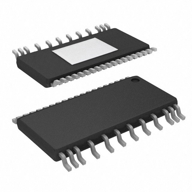
Package
The LT3753HFE#PBF is available in a compact and industry-standard 20-pin TSSOP package. This package provides excellent thermal performance and ease of integration into different circuit designs.
Essence
The essence of LT3753HFE#PBF lies in its ability to efficiently manage power conversion, enabling reliable and optimized operation of electronic systems.
Packaging/Quantity
The IC is typically supplied in tape and reel packaging, with a quantity of 250 units per reel.
Specifications
- Input Voltage Range: 4V to 60V
- Output Voltage Range: 0.8V to 60V
- Maximum Switching Frequency: 1MHz
- Operating Temperature Range: -40°C to 125°C
- Control Interface: SPI (Serial Peripheral Interface)
- Efficiency: Up to 95%
Detailed Pin Configuration
- VIN: Input voltage pin
- GND: Ground reference pin
- VCC: Supply voltage for internal circuitry
- SDI: Serial data input for SPI communication
- SDO: Serial data output for SPI communication
- SCK: Serial clock input for SPI communication
- SYNC: Synchronization input for external clock
- FB: Feedback pin for output voltage regulation
- SS: Chip select input for SPI communication
- EN/UVLO: Enable and undervoltage lockout control pin
- PGND: Power ground reference pin
- SW: Switching node connection for power conversion
- BST: Boost capacitor connection
- LX: Inductor connection for power conversion
- COMP: Compensation pin for stability optimization
- RT/CLKOUT: External resistor connection for frequency adjustment or clock output
- AGND: Analog ground reference pin
- VREF: Reference voltage output
- ADJ: Output voltage adjustment pin
- VOUT: Output voltage pin
Functional Features
- Wide input voltage range allows compatibility with various power sources.
- Flexible output configurations enable versatile power conversion options.
- Adjustable switching frequency provides optimization for different applications.
- Comprehensive protection features ensure safe operation and system reliability.
- SPI interface facilitates easy control and monitoring of the IC.
Advantages and Disadvantages
Advantages
- High efficiency power conversion reduces energy losses.
- Versatile output configurations cater to diverse application needs.
- Compact package enables easy integration into different circuit designs.
- Extensive protection features enhance system safety and reliability.
- Adjustable frequency allows optimization for specific requirements.
Disadvantages
- Limited maximum switching frequency may not be suitable for certain high-frequency applications.
- Requires external components for complete power management solutions.
Working Principles
The LT3753HFE#PBF operates based on a pulse-width modulation (PWM) control scheme. It regulates the power conversion process by adjusting the duty cycle of the switching transistor. This control mechanism ensures that the output voltage remains stable and within the desired range, even with varying input voltages.
The IC incorporates a feedback loop that continuously monitors the output voltage and adjusts the duty cycle accordingly. It also includes various protection circuits to safeguard against overvoltage, overcurrent, and thermal issues.
Detailed Application Field Plans
The LT3753HFE#PBF finds applications in a wide range of electronic systems, including:
- Power supplies for industrial equipment
- Battery chargers for portable devices
- LED drivers for lighting applications
- Automotive power management systems
- Renewable energy systems
- Telecom infrastructure power modules
- Medical equipment power supplies
Detailed and Complete Alternative Models
- LT3753HFE#TRPBF: Similar to LT3753HFE#PBF but supplied in tape and reel packaging with 1500 units per reel.
- LT3753HFE#PBF-ND: Same as LT3753
Перечислите 10 распространенных вопросов и ответов, связанных с применением LT3753HFE#PBF в технических решениях.
Sure! Here are 10 common questions and answers related to the application of LT3753HFE#PBF in technical solutions:
Q: What is the LT3753HFE#PBF? A: The LT3753HFE#PBF is a high voltage, current mode DC/DC controller designed for driving N-channel MOSFETs in boost, SEPIC, flyback, and forward converter topologies.
Q: What is the input voltage range supported by the LT3753HFE#PBF? A: The LT3753HFE#PBF supports an input voltage range from 4V to 100V.
Q: What is the maximum switching frequency of the LT3753HFE#PBF? A: The LT3753HFE#PBF can operate at a maximum switching frequency of 500kHz.
Q: Can the LT3753HFE#PBF be used in automotive applications? A: Yes, the LT3753HFE#PBF is suitable for automotive applications as it operates over a wide temperature range and has built-in protection features.
Q: Does the LT3753HFE#PBF have any integrated protection features? A: Yes, the LT3753HFE#PBF includes features like overvoltage protection, undervoltage lockout, and thermal shutdown.
Q: What is the typical efficiency of the LT3753HFE#PBF? A: The LT3753HFE#PBF can achieve efficiencies of up to 95% depending on the specific application and operating conditions.
Q: Can the LT3753HFE#PBF drive multiple output channels? A: Yes, the LT3753HFE#PBF can drive multiple output channels by using external MOSFETs and transformers.
Q: What is the maximum output current supported by the LT3753HFE#PBF? A: The LT3753HFE#PBF can support output currents up to 20A, depending on the specific application and thermal considerations.
Q: Is there any reference design available for the LT3753HFE#PBF? A: Yes, Linear Technology (now part of Analog Devices) provides reference designs and application notes for the LT3753HFE#PBF on their website.
Q: Can the LT3753HFE#PBF be used in battery charging applications? A: Yes, the LT3753HFE#PBF can be used in battery charging applications by configuring it as a boost or SEPIC converter with appropriate control circuitry.
Please note that these answers are general and may vary depending on the specific requirements and conditions of your application. It is always recommended to refer to the datasheet and application notes provided by the manufacturer for detailed information.