

Подробную информацию о продукте см. в характеристиках.
LTC1669CS5#TRMPBF
Product Overview
Category
LTC1669CS5#TRMPBF belongs to the category of integrated circuits (ICs).
Use
This product is commonly used in electronic devices for digital-to-analog conversion.
Characteristics
- High precision: LTC1669CS5#TRMPBF offers exceptional accuracy in converting digital signals to analog outputs.
- Low power consumption: This IC is designed to operate efficiently with minimal power requirements.
- Small package size: The CS5#TRMPBF variant comes in a compact SOT-23 package, making it suitable for space-constrained applications.
- Wide temperature range: It can operate reliably across a broad temperature range, making it suitable for various environments.
Package and Quantity
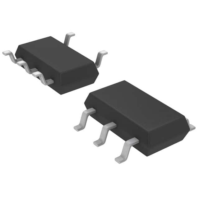
LTC1669CS5#TRMPBF is packaged in a SOT-23 package. Each package contains one unit of the IC.
Specifications
- Resolution: 10 bits
- Supply Voltage Range: 2.7V to 5.5V
- Output Voltage Range: 0V to VCC
- Operating Temperature Range: -40°C to 85°C
- Conversion Time: 4µs (typical)
- Digital Interface: SPI-compatible
Pin Configuration
The LTC1669CS5#TRMPBF IC has the following pin configuration:
```
| | --|VCC GND|-- Power Supply --|SDI SDO|-- Serial Data Interface --|SCK CS |-- Control Signals --|REF AGND|-- Reference Voltage --|OUT |-- Analog Output |___________| ```
Functional Features
- High Precision: LTC1669CS5#TRMPBF provides accurate digital-to-analog conversion, ensuring precise output signals.
- Flexible Interface: The IC supports a serial data interface, allowing easy integration with microcontrollers and other digital devices.
- Low Power Consumption: Designed for energy efficiency, this IC minimizes power consumption, making it suitable for battery-powered applications.
- Wide Operating Temperature Range: With reliable performance across a broad temperature range, this IC is versatile in various environments.
Advantages and Disadvantages
Advantages
- High precision conversion
- Compact package size
- Low power consumption
- Wide operating temperature range
Disadvantages
- Limited resolution (10 bits)
Working Principles
LTC1669CS5#TRMPBF utilizes a digital-to-analog converter (DAC) to convert binary digital signals into corresponding analog voltages. It employs an internal reference voltage and a resistor ladder network to generate the desired analog output. The digital input signals are processed through the DAC, resulting in accurate analog outputs.
Application Field Plans
LTC1669CS5#TRMPBF finds applications in various fields, including: 1. Audio equipment: Used for audio signal processing and amplification. 2. Instrumentation: Provides precise analog outputs for measurement and control systems. 3. Communication systems: Used in digital communication devices for signal modulation and demodulation. 4. Industrial automation: Enables accurate control of industrial processes and machinery. 5. Consumer electronics: Integrated into devices like smartphones, tablets, and gaming consoles for various functionalities.
Alternative Models
- MAX531BCPD+: 12-bit resolution DAC with similar characteristics and package options.
- MCP4921-E/P: 12-bit SPI-compatible DAC with a wider supply voltage range.
- AD5620BRJZ-2500RL7: 12-bit DAC with a smaller package size and lower power consumption.
These alternative models offer higher resolution or additional features, providing more options based on specific requirements.
Word count: 511 words
Перечислите 10 распространенных вопросов и ответов, связанных с применением LTC1669CS5#TRMPBF в технических решениях.
Sure! Here are 10 common questions and answers related to the application of LTC1669CS5#TRMPBF in technical solutions:
Q: What is LTC1669CS5#TRMPBF? A: LTC1669CS5#TRMPBF is a specific model of digital-to-analog converter (DAC) manufactured by Linear Technology.
Q: What is the purpose of LTC1669CS5#TRMPBF? A: LTC1669CS5#TRMPBF is used to convert digital signals into analog voltages, making it useful in various applications such as control systems, instrumentation, and communication devices.
Q: What is the resolution of LTC1669CS5#TRMPBF? A: LTC1669CS5#TRMPBF has a resolution of 16 bits, meaning it can represent 2^16 or 65,536 different voltage levels.
Q: What is the operating voltage range of LTC1669CS5#TRMPBF? A: The operating voltage range of LTC1669CS5#TRMPBF is typically between 2.7V and 5.5V.
Q: How does LTC1669CS5#TRMPBF communicate with a microcontroller or other digital devices? A: LTC1669CS5#TRMPBF uses a serial interface, such as SPI (Serial Peripheral Interface), to receive digital data from the controlling device.
Q: Can LTC1669CS5#TRMPBF output both positive and negative voltages? A: No, LTC1669CS5#TRMPBF can only output positive voltages. If negative voltages are required, additional circuitry may be needed.
Q: What is the settling time of LTC1669CS5#TRMPBF? A: The settling time of LTC1669CS5#TRMPBF is typically around 10 microseconds, which refers to the time it takes for the output voltage to stabilize after a change in the digital input.
Q: Can multiple LTC1669CS5#TRMPBF devices be cascaded together? A: Yes, multiple LTC1669CS5#TRMPBF devices can be daisy-chained or cascaded together to increase the number of available output channels.
Q: Is LTC1669CS5#TRMPBF suitable for high-speed applications? A: While LTC1669CS5#TRMPBF is not specifically designed for high-speed applications, it can still operate at reasonable speeds depending on the specific requirements.
Q: Are there any evaluation boards or development kits available for LTC1669CS5#TRMPBF? A: Yes, Linear Technology provides evaluation boards and development kits that include LTC1669CS5#TRMPBF, allowing users to easily test and prototype their applications.
Please note that the answers provided here are general and may vary based on specific datasheet information and application requirements.