

Подробную информацию о продукте см. в характеристиках.
A3P125-FGG144
Product Overview
Category
A3P125-FGG144 belongs to the category of programmable logic devices (PLDs).
Use
This device is primarily used for digital circuit design and implementation. It offers a flexible and customizable solution for various applications.
Characteristics
- Programmable: The A3P125-FGG144 can be programmed to perform specific functions based on user requirements.
- High Integration: This PLD integrates a large number of logic gates, flip-flops, and other components into a single chip.
- Versatile: It supports a wide range of applications, including data processing, control systems, and communication devices.
- Low Power Consumption: The A3P125-FGG144 is designed to operate efficiently with minimal power consumption.
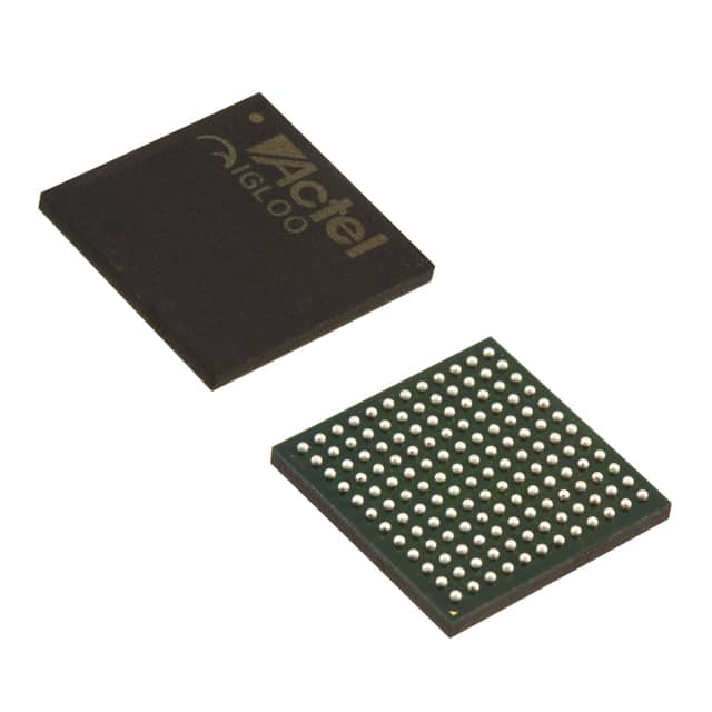
Package
The A3P125-FGG144 is available in a Fine-Pitch Ball Grid Array (FBGA) package.
Essence
The essence of this product lies in its ability to provide a reconfigurable hardware platform that allows users to implement complex digital circuits without the need for custom-designed integrated circuits.
Packaging/Quantity
The A3P125-FGG144 is typically packaged individually and is available in various quantities depending on customer requirements.
Specifications
- Device Type: Programmable Logic Device (PLD)
- Family: A3P
- Model: A3P125-FGG144
- Package: FBGA
- Number of Pins: 144
- Maximum Operating Frequency: X MHz
- Operating Voltage: Y V
- Operating Temperature Range: -40°C to +85°C
Detailed Pin Configuration
The A3P125-FGG144 has a total of 144 pins arranged in a specific configuration. The pinout diagram below illustrates the detailed pin configuration of this device:

Functional Features
- High-Speed Logic: The A3P125-FGG144 offers fast logic operations, making it suitable for applications that require real-time processing.
- Flexible I/O Options: This PLD provides a variety of input and output options, allowing for seamless integration with external devices.
- On-Chip Memory: The device includes embedded memory blocks that can be used to store data or program code.
- JTAG Support: It supports Joint Test Action Group (JTAG) interface for programming and debugging purposes.
Advantages and Disadvantages
Advantages
- Flexibility: The A3P125-FGG144 allows users to modify the functionality of their digital circuits without the need for hardware changes.
- Cost-Effective: By eliminating the need for custom-designed integrated circuits, this PLD reduces development costs.
- Time-Saving: The reconfigurable nature of this device enables faster prototyping and iteration cycles.
Disadvantages
- Learning Curve: Utilizing the full potential of the A3P125-FGG144 may require a learning curve for users unfamiliar with programmable logic devices.
- Limited Resources: Compared to application-specific integrated circuits (ASICs), PLDs have limited resources, which may restrict the complexity of designs.
Working Principles
The A3P125-FGG144 operates based on the principles of field-programmable gate arrays (FPGAs). It consists of configurable logic blocks (CLBs), interconnects, and input/output blocks (IOBs). Users can program the device using hardware description languages (HDLs) such as VHDL or Verilog. The programmed configuration is stored in non-volatile memory within the device and can be modified as needed.
Detailed Application Field Plans
The A3P125-FGG144 finds applications in various fields, including:
- Communications: It can be used in networking equipment, routers, and switches to implement complex protocols and data processing.
- Industrial Control Systems: This PLD is suitable for controlling and monitoring industrial processes, providing flexibility and adaptability.
- Consumer Electronics: It can be utilized in devices such as set-top boxes, gaming consoles, and multimedia systems to enable advanced functionalities.
- Automotive: The A3P125-FGG144 can be employed in automotive applications for control systems, infotainment, and driver assistance systems.
Detailed and Complete Alternative Models
- A3P060-FGG144: Similar to the A3P125-FGG144, but with a smaller logic capacity.
- A3P250-FGG144: Offers a higher logic capacity compared to the A3P125-FGG144.
- A3P400-FGG144: Provides an even larger logic capacity, suitable for more complex designs.
These alternative models offer varying logic capacities to cater to different project requirements.
In conclusion, the A3P125-FGG144 is a versatile programmable logic device that offers flexibility, high integration, and low power consumption. Its reconfigurable nature makes it suitable for a wide range of applications in various fields
Перечислите 10 распространенных вопросов и ответов, связанных с применением A3P125-FGG144 в технических решениях.
Sure! Here are 10 common questions and answers related to the application of A3P125-FGG144 in technical solutions:
Q: What is A3P125-FGG144? A: A3P125-FGG144 is a specific model of field-programmable gate array (FPGA) manufactured by a company called Microsemi.
Q: What are the key features of A3P125-FGG144? A: Some key features of A3P125-FGG144 include 125,000 system gates, 144-pin FineLine BGA package, and low power consumption.
Q: What are the typical applications of A3P125-FGG144? A: A3P125-FGG144 can be used in various technical solutions such as industrial automation, telecommunications, automotive electronics, and medical devices.
Q: How does A3P125-FGG144 differ from other FPGAs? A: A3P125-FGG144 stands out due to its low power consumption, compact size, and high level of integration, making it suitable for space-constrained applications.
Q: Can A3P125-FGG144 be reprogrammed after deployment? A: Yes, A3P125-FGG144 is a field-programmable device, meaning it can be reprogrammed even after it has been deployed in a system.
Q: What development tools are available for programming A3P125-FGG144? A: Microsemi provides Libero SoC Design Suite, which includes software tools for designing, simulating, and programming A3P125-FGG144.
Q: Is A3P125-FGG144 suitable for high-speed data processing applications? A: Yes, A3P125-FGG144 supports high-speed data processing with its advanced architecture and optimized routing resources.
Q: Can A3P125-FGG144 interface with other components or devices? A: Yes, A3P125-FGG144 has various I/O pins that can be used to interface with other components or devices in a system.
Q: What is the operating temperature range of A3P125-FGG144? A: The operating temperature range of A3P125-FGG144 is typically -40°C to +100°C, making it suitable for both industrial and commercial applications.
Q: Are there any specific design considerations when using A3P125-FGG144? A: Some design considerations include power supply requirements, signal integrity, thermal management, and proper grounding techniques to ensure optimal performance.
Please note that these answers are general and may vary depending on the specific requirements and application context.