

Подробную информацию о продукте см. в характеристиках.
Encyclopedia Entry: 74AUP3G07GSX
Product Overview
Category
The 74AUP3G07GSX belongs to the category of integrated circuits (ICs).
Use
This IC is commonly used in electronic devices for signal amplification and buffering purposes.
Characteristics
- Low power consumption
- High-speed operation
- Wide operating voltage range
- Small package size
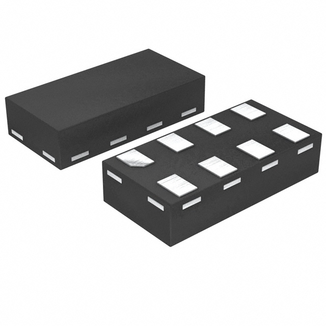
Package
The 74AUP3G07GSX is available in a small outline package (SOT) with three pins.
Essence
The essence of this product lies in its ability to amplify and buffer signals efficiently while consuming minimal power.
Packaging/Quantity
The 74AUP3G07GSX is typically packaged in reels or tubes, with a quantity of 3000 units per reel/tube.
Specifications
- Supply Voltage Range: 1.65V to 5.5V
- Input Voltage Range: -0.5V to VCC + 0.5V
- Output Voltage Range: -0.5V to VCC + 0.5V
- Operating Temperature Range: -40°C to +85°C
- Maximum Power Dissipation: 150mW
Detailed Pin Configuration
The 74AUP3G07GSX has three pins arranged as follows:
```
| | --| 1 2 |-- --| |-- --| 3 |-- |___________| ```
Pin 1: Input A Pin 2: Output Y Pin 3: GND (Ground)
Functional Features
- Signal amplification: The 74AUP3G07GSX amplifies weak input signals to a higher level.
- Signal buffering: It provides impedance matching and isolates the input and output signals.
- High-speed operation: This IC operates at high speeds, making it suitable for applications requiring quick signal processing.
Advantages and Disadvantages
Advantages
- Low power consumption: The 74AUP3G07GSX is designed to minimize power usage, making it energy-efficient.
- Wide operating voltage range: It can operate within a broad voltage range, providing flexibility in various applications.
- Small package size: The compact size of this IC allows for space-saving designs in electronic devices.
Disadvantages
- Limited output current: The 74AUP3G07GSX has a relatively low output current capability, which may restrict its use in certain applications.
- Sensitivity to electrostatic discharge (ESD): Care must be taken during handling and installation to prevent damage from ESD.
Working Principles
The 74AUP3G07GSX utilizes a combination of transistors and resistors to amplify and buffer input signals. When an input signal is applied, the internal circuitry amplifies it to a higher level while maintaining signal integrity. The buffered output signal is then available for further processing or transmission.
Detailed Application Field Plans
The 74AUP3G07GSX finds application in various electronic devices and systems, including:
- Mobile phones: Signal amplification and buffering in audio circuits.
- Computers: Interface signal conditioning for data transmission.
- Automotive electronics: Amplification and buffering of sensor signals.
- Consumer electronics: Signal processing in audio/video equipment.
Detailed and Complete Alternative Models
- 74LVC07APW: Similar functionality with different voltage specifications.
- SN74LV1T34DBVR: Single-channel buffer with comparable characteristics.
- MC74VHC1GT50DTT1G: Voltage level translator with buffering capabilities.
These alternative models offer similar features and can be used as substitutes for the 74AUP3G07GSX in various applications.
Word count: 526 words
Перечислите 10 распространенных вопросов и ответов, связанных с применением 74AUP3G07GSX в технических решениях.
Sure! Here are 10 common questions and answers related to the application of 74AUP3G07GSX in technical solutions:
Q: What is the 74AUP3G07GSX? A: The 74AUP3G07GSX is a triple buffer/driver IC (integrated circuit) that can be used for level shifting and signal buffering in various electronic applications.
Q: What is the voltage range supported by the 74AUP3G07GSX? A: The 74AUP3G07GSX supports a wide voltage range from 0.8V to 3.6V, making it compatible with many different logic families.
Q: Can the 74AUP3G07GSX be used as a voltage level shifter? A: Yes, the 74AUP3G07GSX can be used as a voltage level shifter to convert signals between different voltage domains.
Q: How many buffers/drivers are there in the 74AUP3G07GSX? A: The 74AUP3G07GSX has three independent buffers/drivers, allowing it to handle multiple signals simultaneously.
Q: What is the maximum output current of the 74AUP3G07GSX? A: The 74AUP3G07GSX can source/sink up to 32mA of current per channel, making it suitable for driving various loads.
Q: Is the 74AUP3G07GSX compatible with both CMOS and TTL logic levels? A: Yes, the 74AUP3G07GSX is compatible with both CMOS and TTL logic levels, providing flexibility in interfacing with different devices.
Q: Can the 74AUP3G07GSX be used in battery-powered applications? A: Yes, the 74AUP3G07GSX has a low power consumption and can operate at lower supply voltages, making it suitable for battery-powered applications.
Q: What is the typical propagation delay of the 74AUP3G07GSX? A: The typical propagation delay of the 74AUP3G07GSX is around 2.5ns, allowing for fast signal transmission.
Q: Does the 74AUP3G07GSX have built-in ESD protection? A: Yes, the 74AUP3G07GSX has built-in ESD (electrostatic discharge) protection, ensuring robustness against static electricity.
Q: Can the 74AUP3G07GSX be used in high-speed data communication applications? A: Yes, the 74AUP3G07GSX has a high bandwidth and can be used in high-speed data communication applications such as USB or HDMI interfaces.
Please note that these answers are general and may vary depending on specific application requirements.