

Подробную информацию о продукте см. в характеристиках.
74AVC8T245BQ-Q100J
Basic Information Overview
- Category: Integrated Circuit (IC)
- Use: Level Shifter and Bus Transceiver
- Characteristics: High-speed, low-voltage, bidirectional voltage level translation
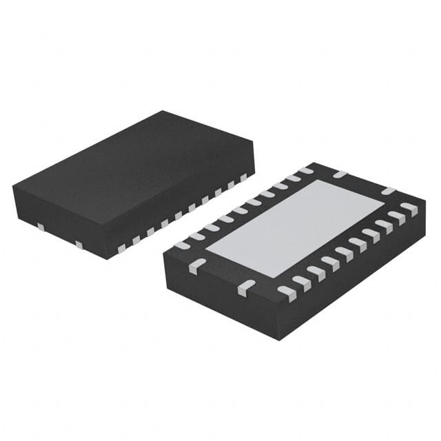
- Package: 48-pin TSSOP (Thin Shrink Small Outline Package)
- Essence: Translates signals between two different voltage domains
- Packaging/Quantity: Tape and Reel, 2500 units per reel
Specifications
- Supply Voltage Range: 1.2V to 3.6V
- Input Voltage Range: 0V to VCC
- Output Voltage Range: 0V to VCC
- Maximum Data Rate: 400 Mbps
- Number of Channels: 8
- Input/Output Type: CMOS/TTL compatible
Detailed Pin Configuration
The 74AVC8T245BQ-Q100J has a total of 48 pins. The pin configuration is as follows:
- OE (Output Enable) 1
- A1 (Data Input/Output) 1
- B1 (Data Input/Output) 1
- GND (Ground)
- B2 (Data Input/Output) 2
- A2 (Data Input/Output) 2
- VCC (Supply Voltage)
- OE (Output Enable) 2
- A3 (Data Input/Output) 3
- B3 (Data Input/Output) 3
- A4 (Data Input/Output) 4
- B4 (Data Input/Output) 4
- A5 (Data Input/Output) 5
- B5 (Data Input/Output) 5
- A6 (Data Input/Output) 6
- B6 (Data Input/Output) 6
- A7 (Data Input/Output) 7
- B7 (Data Input/Output) 7
- A8 (Data Input/Output) 8
- B8 (Data Input/Output) 8
- VCC (Supply Voltage)
- GND (Ground)
- DIR (Direction Control)
- GND (Ground)
- B1 (Data Input/Output) 1
- A1 (Data Input/Output) 1
- OE (Output Enable) 1
- VCC (Supply Voltage)
- A2 (Data Input/Output) 2
- B2 (Data Input/Output) 2
- GND (Ground)
- B3 (Data Input/Output) 3
- A3 (Data Input/Output) 3
- B4 (Data Input/Output) 4
- A4 (Data Input/Output) 4
- B5 (Data Input/Output) 5
- A5 (Data Input/Output) 5
- B6 (Data Input/Output) 6
- A6 (Data Input/Output) 6
- B7 (Data Input/Output) 7
- A7 (Data Input/Output) 7
- B8 (Data Input/Output) 8
- A8 (Data Input/Output) 8
- GND (Ground)
- VCC (Supply Voltage)
- DIR (Direction Control)
- GND (Ground)
- NC (No Connection)
Functional Features
- Bidirectional voltage level translation between two voltage domains
- Automatic direction control based on DIR pin
- High-speed data transmission up to 400 Mbps
- Low-voltage operation from 1.2V to 3.6V
- CMOS/TTL compatible input/output levels
Advantages and Disadvantages
Advantages: - Enables communication between devices operating at different voltage levels - Supports high-speed data transmission - Compact package size for space-constrained applications
Disadvantages: - Requires careful consideration of voltage compatibility and signal integrity
Working Principles
The 74AVC8T245BQ-Q100J is a bidirectional level shifter and bus transceiver. It translates signals between two voltage domains, allowing communication between devices operating at different voltage levels. The direction of data flow is controlled by the DIR pin. The IC operates at high speeds and supports data rates up to 400 Mbps. It is designed to work with low-voltage systems, ranging from 1.2V to 3.6V.
Detailed Application Field Plans
The 74AVC8T245BQ-Q100J is commonly used in various applications where voltage level translation is required. Some of the typical
Перечислите 10 распространенных вопросов и ответов, связанных с применением 74AVC8T245BQ-Q100J в технических решениях.
Sure! Here are 10 common questions and answers related to the application of 74AVC8T245BQ-Q100J in technical solutions:
Question: What is the 74AVC8T245BQ-Q100J?
Answer: The 74AVC8T245BQ-Q100J is a bidirectional octal voltage level translator with 3-state outputs.Question: What is the voltage range supported by the 74AVC8T245BQ-Q100J?
Answer: The 74AVC8T245BQ-Q100J supports voltage translation from 1.2V to 3.6V on the A-side and 1.65V to 5.5V on the B-side.Question: How many channels does the 74AVC8T245BQ-Q100J have?
Answer: The 74AVC8T245BQ-Q100J has 8 bidirectional channels.Question: Can the 74AVC8T245BQ-Q100J handle high-speed data transmission?
Answer: Yes, the 74AVC8T245BQ-Q100J is designed for high-speed data transmission up to 400 Mbps.Question: Is the 74AVC8T245BQ-Q100J compatible with I2C and SPI interfaces?
Answer: Yes, the 74AVC8T245BQ-Q100J can be used for voltage level translation in I2C and SPI interfaces.Question: Does the 74AVC8T245BQ-Q100J support hot-swapping?
Answer: No, the 74AVC8T245BQ-Q100J does not support hot-swapping. It is recommended to power down the device before connecting or disconnecting signals.Question: What is the maximum current that can be sourced/sunk by each channel?
Answer: Each channel of the 74AVC8T245BQ-Q100J can source/sink up to 32 mA.Question: Can the 74AVC8T245BQ-Q100J be used in automotive applications?
Answer: Yes, the 74AVC8T245BQ-Q100J is qualified for automotive applications and meets the AEC-Q100 standard.Question: Is there any special consideration for power supply decoupling?
Answer: Yes, it is recommended to use a decoupling capacitor (typically 0.1 µF) between VCCA and GND, as well as between VCCB and GND.Question: Are there any specific layout guidelines for using the 74AVC8T245BQ-Q100J?
Answer: Yes, it is important to follow the recommended layout guidelines provided in the datasheet to minimize noise and ensure proper signal integrity.
Please note that these answers are general and may vary depending on the specific application and requirements. It is always recommended to refer to the datasheet and consult with the manufacturer for detailed information.