

Подробную информацию о продукте см. в характеристиках.
74LVC1G125GV,125
Basic Information Overview
- Category: Integrated Circuit (IC)
- Use: Buffer/Driver
- Characteristics: Low Voltage CMOS, Single Gate, Non-Inverting
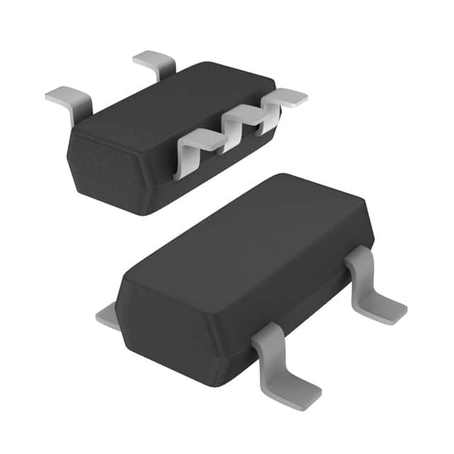
- Package: SOT753 (SC-70)
- Essence: Logic Level Shifter
- Packaging/Quantity: Tape and Reel, 3000 pieces per reel
Specifications
- Supply Voltage Range: 1.65V to 5.5V
- High-Level Input Voltage: 0.7 x VCC
- Low-Level Input Voltage: 0.3 x VCC
- High-Level Output Voltage: 0.9 x VCC
- Low-Level Output Voltage: 0.1 x VCC
- Maximum Output Current: ±32mA
- Propagation Delay: 4.3ns (typical) at 3.3V
- Operating Temperature Range: -40°C to +125°C
Detailed Pin Configuration
The 74LVC1G125GV,125 has a total of 5 pins: 1. GND (Ground) 2. A (Input) 3. OE (Output Enable) 4. Y (Output) 5. VCC (Power Supply)
Functional Features
- Non-inverting buffer/driver with 3-state output
- Provides level shifting between different voltage domains
- Supports bidirectional communication
- Allows multiple devices to share a common bus
Advantages
- Wide supply voltage range allows compatibility with various systems
- Low power consumption
- Fast propagation delay ensures efficient signal transmission
- Small package size enables space-saving designs
- 3-state output allows for easy bus sharing
Disadvantages
- Limited output current may not be suitable for high-power applications
- Single gate configuration restricts the number of inputs/outputs
Working Principles
The 74LVC1G125GV,125 is based on CMOS technology and operates as a non-inverting buffer/driver. It takes the input signal from pin A and amplifies it to the output pin Y. The OE pin controls the output enable/disable state. When OE is low, the output is enabled and follows the input signal. When OE is high, the output is in a high-impedance state (3-state), allowing other devices to drive the bus.
Detailed Application Field Plans
The 74LVC1G125GV,125 is commonly used in various applications, including: - Level shifting between different voltage domains in mixed-signal systems - Buffering and driving signals in communication interfaces (UART, SPI, I2C) - Enabling bidirectional communication on shared buses (such as I2C or SMBus) - Signal conditioning and amplification in sensor interfaces
Detailed and Complete Alternative Models
Some alternative models that can be considered as replacements for the 74LVC1G125GV,125 are: - SN74LVC1G125DBVR (Texas Instruments) - MC74VHC1GT125DF1G (ON Semiconductor) - NCV8181DR2G (ON Semiconductor) - TC7SZ125FU(TE85L,F) (Toshiba)
Note: These alternative models may have slightly different specifications and package options. It is important to review their datasheets for compatibility with specific requirements.
Word count: 365 words
Перечислите 10 распространенных вопросов и ответов, связанных с применением 74LVC1G125GV,125 в технических решениях.
Sure! Here are 10 common questions and answers related to the application of 74LVC1G125GV,125 in technical solutions:
Q1: What is the 74LVC1G125GV,125? A1: The 74LVC1G125GV,125 is a single bus buffer gate with 3-state output. It is commonly used in digital logic circuits.
Q2: What is the voltage range supported by 74LVC1G125GV,125? A2: The 74LVC1G125GV,125 supports a voltage range from 1.65V to 5.5V.
Q3: What is the maximum output current of 74LVC1G125GV,125? A3: The maximum output current of 74LVC1G125GV,125 is typically 32mA.
Q4: Can I use 74LVC1G125GV,125 for level shifting between different voltage domains? A4: Yes, the 74LVC1G125GV,125 can be used for level shifting between different voltage domains due to its wide voltage range support.
Q5: How many inputs does 74LVC1G125GV,125 have? A5: The 74LVC1G125GV,125 has one input.
Q6: Can I connect multiple 74LVC1G125GV,125 devices together to drive a common bus? A6: Yes, you can connect multiple 74LVC1G125GV,125 devices together to drive a common bus.
Q7: Does 74LVC1G125GV,125 have any internal pull-up or pull-down resistors? A7: No, the 74LVC1G125GV,125 does not have any internal pull-up or pull-down resistors.
Q8: What is the propagation delay of 74LVC1G125GV,125? A8: The propagation delay of 74LVC1G125GV,125 is typically around 4.3ns.
Q9: Can I use 74LVC1G125GV,125 for bidirectional communication? A9: No, the 74LVC1G125GV,125 is a unidirectional buffer and does not support bidirectional communication.
Q10: Is 74LVC1G125GV,125 available in different package options? A10: Yes, 74LVC1G125GV,125 is available in various package options such as SOT23, SC-70, and XSON.