

Подробную информацию о продукте см. в характеристиках.
74LVCH162373ADL:11
Basic Information Overview
- Category: Integrated Circuit (IC)
- Use: Data storage and transfer
- Characteristics: High-speed, low-voltage, 16-bit transparent latch/flip-flop with 3-state outputs
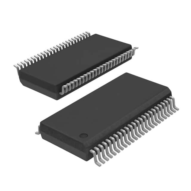
- Package: TSSOP (Thin Shrink Small Outline Package)
- Essence: The 74LVCH162373ADL:11 is a latch/flip-flop IC that allows for the storage and transfer of data in digital systems. It operates at high speeds and low voltages, making it suitable for various applications.
- Packaging/Quantity: Available in reels or tubes, typically containing 250 to 300 units per package.
Specifications
- Logic Family: LVCH
- Number of Bits: 16
- Output Type: 3-state
- Supply Voltage Range: 1.2V to 3.6V
- Operating Temperature Range: -40°C to +85°C
- Input/Output Compatibility: TTL, CMOS
Detailed Pin Configuration
The 74LVCH162373ADL:11 has a total of 48 pins, which are divided into three groups: - Group A (pins 1-24): Inputs/outputs for latch control and data transfer - Group B (pins 25-36): Inputs/outputs for data inputs and outputs - Group C (pins 37-48): Power supply and ground pins
Functional Features
- Transparent Latch/Flip-Flop: Allows for the storage and transfer of data between input and output ports.
- 3-State Outputs: Provides the ability to disconnect the outputs from the bus, allowing multiple devices to share the same bus without interference.
- High-Speed Operation: Enables fast data transfer within digital systems.
- Low-Voltage Operation: Supports operation at low power supply voltages, reducing power consumption.
Advantages and Disadvantages
Advantages: - High-speed operation allows for efficient data transfer. - Low-voltage operation reduces power consumption. - 3-state outputs enable bus sharing among multiple devices.
Disadvantages: - Limited number of bits (16) may not be suitable for applications requiring larger data storage capacity. - TSSOP package may require careful handling during assembly.
Working Principles
The 74LVCH162373ADL:11 operates based on the principles of latch/flip-flop circuits. It uses transparent latches to store and transfer data between input and output ports. The latch control inputs determine whether the data is stored or transferred. The 3-state outputs allow the device to disconnect from the bus when necessary, preventing interference with other devices.
Detailed Application Field Plans
The 74LVCH162373ADL:11 can be used in various digital systems that require data storage and transfer capabilities. Some potential application fields include: - Microcontrollers and microprocessors - Communication systems - Data acquisition systems - Industrial automation - Automotive electronics
Detailed and Complete Alternative Models
- 74HC373: Similar latch/flip-flop IC with 8-bit capacity, compatible with CMOS and TTL logic levels.
- SN74LVC162373A: 16-bit transparent latch/flip-flop with 3-state outputs, compatible with a wide range of supply voltages.
- CD54HC373: Octal transparent latch/flip-flop with 3-state outputs, compatible with high-speed CMOS logic.
(Note: The above alternative models are provided as examples and may not cover all available options.)
This entry provides an overview of the 74LVCH162373ADL:11 integrated circuit, including its basic information, specifications, pin configuration, functional features, advantages and disadvantages, working principles, application field plans, and alternative models.
Перечислите 10 распространенных вопросов и ответов, связанных с применением 74LVCH162373ADL:11 в технических решениях.
Sure! Here are 10 common questions and answers related to the application of 74LVCH162373ADL:11 in technical solutions:
Q: What is the function of the 74LVCH162373ADL:11?
A: The 74LVCH162373ADL:11 is a 16-bit transparent latch with 3-state outputs.Q: What is the voltage supply range for this device?
A: The voltage supply range for the 74LVCH162373ADL:11 is typically between 1.65V and 3.6V.Q: How many latch outputs does this device have?
A: The 74LVCH162373ADL:11 has 16 latch outputs.Q: Can I use this device for level shifting applications?
A: Yes, the 74LVCH162373ADL:11 can be used for level shifting as it supports both 3.3V and 5V logic levels.Q: What is the maximum data transfer rate supported by this device?
A: The 74LVCH162373ADL:11 can support data transfer rates up to 400Mbps.Q: Does this device have any built-in ESD protection?
A: Yes, the 74LVCH162373ADL:11 has built-in ESD protection, making it more robust against electrostatic discharge.Q: Can I cascade multiple 74LVCH162373ADL:11 devices together?
A: Yes, you can cascade multiple devices to increase the number of latch outputs.Q: What is the power consumption of this device?
A: The power consumption of the 74LVCH162373ADL:11 is typically low, making it suitable for power-sensitive applications.Q: Can I use this device in both parallel and serial data transfer applications?
A: Yes, the 74LVCH162373ADL:11 can be used for both parallel and serial data transfer applications.Q: Are there any specific timing requirements for using this device?
A: Yes, the 74LVCH162373ADL:11 has specific setup and hold time requirements that need to be met for reliable operation.
Please note that these answers are general and may vary depending on the specific application and requirements. It's always recommended to refer to the device datasheet and consult with the manufacturer for detailed information.