

Подробную информацию о продукте см. в характеристиках.
Encyclopedia Entry: 74ACT374MTC
Product Overview
- Category: Integrated Circuit (IC)
- Use: Flip-Flop / Latch
- Characteristics: High-speed, low-power consumption
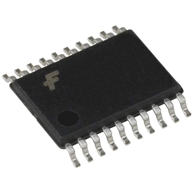
- Package: TSSOP (Thin Shrink Small Outline Package)
- Essence: Octal D-type flip-flop with 3-state outputs
- Packaging/Quantity: Tape and Reel, 2500 units per reel
Specifications
- Supply Voltage: 2.0V to 6.0V
- Input Voltage: 0V to VCC
- Output Voltage: 0V to VCC
- Operating Temperature: -40°C to +85°C
- Propagation Delay: 4.5ns (typical)
- Output Drive Capability: ±24mA
Detailed Pin Configuration
The 74ACT374MTC IC has a total of 20 pins, which are assigned as follows:
- Pin 1: Output Enable (OE)
- Pin 2: Data Input (D0)
- Pin 3: Data Input (D1)
- Pin 4: Data Input (D2)
- Pin 5: Data Input (D3)
- Pin 6: Data Input (D4)
- Pin 7: Data Input (D5)
- Pin 8: Data Input (D6)
- Pin 9: Data Input (D7)
- Pin 10: Clock Input (CLK)
- Pin 11: Master Reset (MR)
- Pin 12: Q Output (Q0)
- Pin 13: Q Output (Q1)
- Pin 14: Q Output (Q2)
- Pin 15: Q Output (Q3)
- Pin 16: Q Output (Q4)
- Pin 17: Q Output (Q5)
- Pin 18: Q Output (Q6)
- Pin 19: Q Output (Q7)
- Pin 20: Ground (GND)
Functional Features
- Octal D-type flip-flop with 3-state outputs
- High-speed operation, suitable for applications requiring quick data storage and retrieval
- Low-power consumption, making it ideal for battery-powered devices
- 3-state outputs allow multiple ICs to be connected together without bus contention issues
Advantages and Disadvantages
Advantages: - High-speed operation enables efficient data processing - Low-power consumption prolongs battery life in portable devices - 3-state outputs facilitate bus sharing in complex systems
Disadvantages: - Limited output drive capability may not be suitable for high-current applications - Requires careful consideration of clock timing to avoid data corruption
Working Principles
The 74ACT374MTC is a positive-edge-triggered flip-flop that stores data on the rising edge of the clock signal. When the master reset (MR) input is low, the flip-flop is enabled, and the data inputs (D0-D7) are transferred to the corresponding Q outputs (Q0-Q7). The output enable (OE) input controls the 3-state outputs, allowing them to be either active or in a high-impedance state.
Detailed Application Field Plans
The 74ACT374MTC is widely used in various digital systems where data storage and retrieval are required. Some common application fields include: - Microprocessors and microcontrollers - Data communication systems - Memory modules - Industrial automation equipment - Automotive electronics
Detailed and Complete Alternative Models
- 74HC374: Similar octal D-type flip-flop with 3-state outputs, but operates at a lower voltage range (2.0V to 6.0V)
- 74LS374: Octal D-type flip-flop with 3-state outputs, compatible with TTL logic levels
- CD74ACT374: Octal D-type flip-flop with 3-state outputs, manufactured by Texas Instruments
(Note: The above alternative models are just a few examples and not an exhaustive list.)
Word Count: 445 words
Перечислите 10 распространенных вопросов и ответов, связанных с применением 74ACT374MTC в технических решениях.
Sure! Here are 10 common questions and answers related to the application of 74ACT374MTC in technical solutions:
Q: What is the 74ACT374MTC? A: The 74ACT374MTC is a type of octal D-type flip-flop integrated circuit (IC) that can store and transfer data in digital systems.
Q: What is the purpose of the 74ACT374MTC? A: The 74ACT374MTC is commonly used for data storage, synchronization, and signal buffering in various digital applications.
Q: How many flip-flops are there in the 74ACT374MTC? A: The 74ACT374MTC consists of eight individual D-type flip-flops, making it an octal flip-flop IC.
Q: What is the voltage range supported by the 74ACT374MTC? A: The 74ACT374MTC operates within a voltage range of 2.0V to 5.5V, making it compatible with both TTL and CMOS logic levels.
Q: Can the 74ACT374MTC handle high-speed data transfers? A: Yes, the 74ACT374MTC is designed to operate at high speeds, with a maximum propagation delay of 6 ns.
Q: How can I connect inputs and outputs to the 74ACT374MTC? A: Inputs are connected to the D (data) pins, while outputs are obtained from the Q (output) pins of each flip-flop.
Q: Can the 74ACT374MTC be cascaded to increase the number of flip-flops? A: Yes, multiple 74ACT374MTC ICs can be cascaded together to increase the number of flip-flops and achieve larger data storage.
Q: What is the clock input used for in the 74ACT374MTC? A: The clock input (CLK) is used to control the timing of data transfers and synchronization within the flip-flops.
Q: Can the 74ACT374MTC be used in both synchronous and asynchronous applications? A: Yes, the 74ACT374MTC supports both synchronous and asynchronous operation modes, depending on how the clock input is used.
Q: Are there any special considerations when using the 74ACT374MTC? A: It is important to ensure proper power supply decoupling and signal integrity measures, such as avoiding excessive noise and maintaining appropriate voltage levels, to ensure reliable operation of the 74ACT374MTC in technical solutions.
Please note that these questions and answers are general in nature and may vary depending on specific application requirements.