

Подробную информацию о продукте см. в характеристиках.
74LCX162374MEA
Basic Information Overview
- Category: Integrated Circuit (IC)
- Use: Data storage and transfer
- Characteristics:
- Low voltage operation
- High-speed performance
- Wide operating temperature range
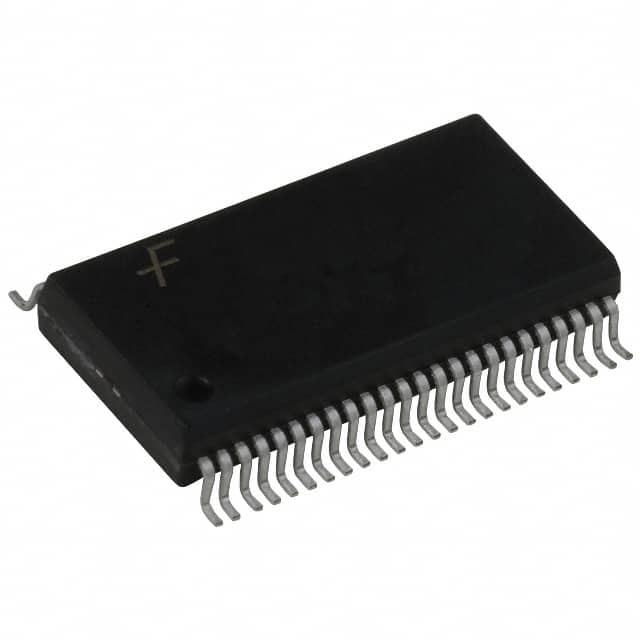
- Package: 48-pin TSSOP (Thin Shrink Small Outline Package)
- Essence: Flip-flop based data storage and transfer IC
- Packaging/Quantity: Available in reels, 2500 units per reel
Specifications
- Supply Voltage: 1.65V to 3.6V
- Input/Output Voltage Levels: 5V tolerant
- Operating Temperature Range: -40°C to +85°C
- Output Drive Capability: ±24mA
- Propagation Delay: 2.5ns (max)
- Output Transition Time: 2.5ns (max)
Detailed Pin Configuration
The 74LCX162374MEA has a total of 48 pins, which are divided into four groups of 12 pins each. The pin configuration is as follows:
Group A (Pins 1-12)
- Output Enable (OE)
- Data Input (D1)
- Data Input (D2)
- Data Input (D3)
- Data Input (D4)
- Data Input (D5)
- Data Input (D6)
- Data Input (D7)
- Data Input (D8)
- Data Input (D9)
- Data Input (D10)
- Data Input (D11)
Group B (Pins 13-24)
- Data Input (D12)
- Data Input (D13)
- Data Input (D14)
- Data Input (D15)
- Data Input (D16)
- Data Input (D17)
- Data Input (D18)
- Data Input (D19)
- Data Input (D20)
- Data Input (D21)
- Data Input (D22)
- Data Input (D23)
Group C (Pins 25-36)
- Data Input (D24)
- Data Input (D25)
- Data Input (D26)
- Data Input (D27)
- Data Input (D28)
- Data Input (D29)
- Data Input (D30)
- Data Input (D31)
- Data Input (D32)
- Data Input (D33)
- Data Input (D34)
- Data Input (D35)
Group D (Pins 37-48)
- Data Input (D36)
- Data Input (D37)
- Data Input (D38)
- Data Input (D39)
- Data Input (D40)
- Data Input (D41)
- Data Input (D42)
- Data Input (D43)
- Data Input (D44)
- Data Input (D45)
- Data Input (D46)
- Data Input (D47)
Functional Features
- 16-bit flip-flop based data storage and transfer
- Non-inverting outputs
- 3-state output capability
- Output enable control for bus-oriented applications
- High-speed operation with low power consumption
- Compatible with various logic families
Advantages and Disadvantages
Advantages: - Low voltage operation allows for compatibility with modern electronic systems - High-speed performance enables efficient data transfer - Wide operating temperature range makes it suitable for various environments - 3-state output capability facilitates bus-oriented applications
Disadvantages: - Limited number of input/output pins may restrict the complexity of applications - Requires external components for proper functioning in a system
Working Principles
The 74LCX162374MEA is based on flip-flop circuits, which are used for storing and transferring digital data. It operates on low voltage and provides high-speed performance. The IC has non-inverting outputs and supports 3-state output capability, making it suitable for bus-oriented applications. By controlling the output enable pin, the IC can be enabled or disabled, allowing for efficient data transfer.
Detailed Application Field Plans
The 74LCX162374MEA finds applications in various fields where data storage and transfer are required. Some of the detailed application field plans include:
- Communication Systems: Used for data buffering and signal transmission in communication networks.
- Computer Systems: Employed in memory modules and data buses for efficient data transfer.
- Industrial Automation: Utilized in control systems for storing and transferring sensor data.
- Automotive Electronics: Integrated into automotive control units for data processing and communication.
- Consumer Electronics: Incorporated in devices like smartphones, tablets, and gaming consoles for data storage and transfer.
Detailed and Complete Alternative Models
Перечислите 10 распространенных вопросов и ответов, связанных с применением 74LCX162374MEA в технических решениях.
Sure! Here are 10 common questions and answers related to the application of 74LCX162374MEA in technical solutions:
Q: What is the 74LCX162374MEA? A: The 74LCX162374MEA is a 16-bit D-type flip-flop with 3-state outputs, commonly used in digital logic circuits.
Q: What is the purpose of the 74LCX162374MEA? A: The purpose of this IC is to store and control the state of 16 bits of data in a digital system.
Q: What voltage levels does the 74LCX162374MEA support? A: The 74LCX162374MEA supports both 3.3V and 5V voltage levels, making it compatible with a wide range of systems.
Q: How many flip-flops are there in the 74LCX162374MEA? A: There are 16 individual flip-flops in the 74LCX162374MEA, each capable of storing one bit of data.
Q: Can I connect multiple 74LCX162374MEA ICs together? A: Yes, you can connect multiple 74LCX162374MEA ICs together to increase the number of bits that can be stored and controlled.
Q: What are the 3-state outputs in the 74LCX162374MEA used for? A: The 3-state outputs allow the IC to be connected to a bus or shared line, enabling multiple devices to drive the same line without conflicts.
Q: What is the maximum clock frequency supported by the 74LCX162374MEA? A: The maximum clock frequency supported by the 74LCX162374MEA is typically specified by the manufacturer and can vary, but it is commonly in the range of several hundred megahertz.
Q: Can I use the 74LCX162374MEA in both synchronous and asynchronous systems? A: Yes, the 74LCX162374MEA can be used in both synchronous and asynchronous systems, depending on how the clock input is connected.
Q: What is the power supply voltage range for the 74LCX162374MEA? A: The power supply voltage range for the 74LCX162374MEA is typically between 2.7V and 3.6V.
Q: Are there any special considerations when using the 74LCX162374MEA in high-speed applications? A: Yes, in high-speed applications, it is important to consider signal integrity, proper decoupling, and minimizing trace lengths to avoid issues like signal skew and noise interference.
Please note that these answers are general and may vary based on specific datasheet specifications and application requirements.