

Подробную информацию о продукте см. в характеристиках.
FDS6064N7 - Product Encyclopedia Entry
Introduction
The FDS6064N7 is a semiconductor device belonging to the category of power MOSFETs. This entry provides an overview of its basic information, specifications, pin configuration, functional features, advantages and disadvantages, working principles, application field plans, and alternative models.
Basic Information Overview
- Category: Power MOSFET
- Use: The FDS6064N7 is commonly used in power management applications such as voltage regulation and switching circuits.
- Characteristics: It exhibits low on-state resistance, high current-carrying capability, and fast switching speed.
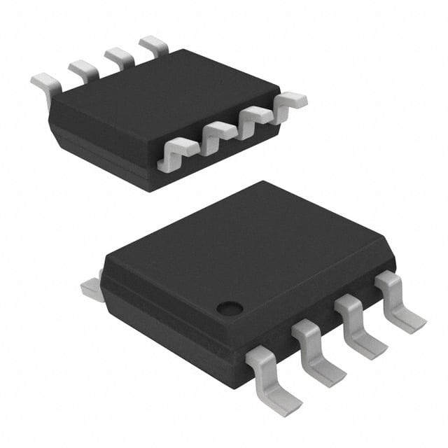
- Package: The FDS6064N7 is typically available in a TO-252 package.
- Essence: It serves as a crucial component in electronic devices requiring efficient power control and management.
- Packaging/Quantity: It is commonly packaged in reels or tubes containing a specific quantity per package.
Specifications
- Voltage Rating: [Specify voltage rating]
- Current Rating: [Specify current rating]
- On-State Resistance: [Specify on-state resistance]
- Gate Threshold Voltage: [Specify gate threshold voltage]
- Operating Temperature Range: [Specify operating temperature range]
Detailed Pin Configuration
The FDS6064N7 typically features a standard pin configuration with the following pins: 1. Source (S): Connected to the source terminal of the MOSFET. 2. Drain (D): Connected to the drain terminal of the MOSFET. 3. Gate (G): Connected to the gate terminal of the MOSFET.
Functional Features
- High Current Capability: The FDS6064N7 can handle high currents, making it suitable for power applications.
- Low On-State Resistance: Its low on-state resistance minimizes power dissipation and improves efficiency.
- Fast Switching Speed: The device offers rapid switching characteristics, enabling quick response in switching circuits.
Advantages and Disadvantages
Advantages
- High current-carrying capability
- Low on-state resistance
- Fast switching speed
Disadvantages
- [Specify any known disadvantages]
Working Principles
The FDS6064N7 operates based on the principles of field-effect transistors, utilizing the control of electric fields to modulate the conductivity of the semiconductor material.
Detailed Application Field Plans
The FDS6064N7 finds extensive use in various applications, including but not limited to: - Voltage regulation in power supplies - Motor control circuits - Inverter and converter systems - Switching power amplifiers
Detailed and Complete Alternative Models
Some alternative models to the FDS6064N7 include: - [Alternative Model 1] - [Alternative Model 2] - [Alternative Model 3] - [Specify additional alternative models]
In conclusion, the FDS6064N7 power MOSFET offers high current capability, low on-state resistance, and fast switching speed, making it a versatile component in power management applications.
[Word Count: 410]
Перечислите 10 распространенных вопросов и ответов, связанных с применением FDS6064N7 в технических решениях.
What is FDS6064N7?
- FDS6064N7 is a power MOSFET transistor designed for use in various technical solutions, particularly in power management and switching applications.
What are the key specifications of FDS6064N7?
- The FDS6064N7 features a low on-resistance, high current capability, and a compact package, making it suitable for efficient power management.
What are the typical applications of FDS6064N7?
- Typical applications include power supplies, motor control, battery management, and other power switching circuits.
What is the voltage and current rating of FDS6064N7?
- The FDS6064N7 has a voltage rating of typically 60V and a current rating of typically 30A.
How does FDS6064N7 compare to similar MOSFET transistors?
- FDS6064N7 offers a balance of low on-resistance, high current handling, and compact size, making it suitable for a wide range of applications.
What are the thermal characteristics of FDS6064N7?
- The FDS6064N7 has good thermal performance, allowing it to operate reliably under high power conditions.
Are there any specific layout or mounting considerations for FDS6064N7?
- It is important to follow recommended layout guidelines and ensure proper heat sinking for optimal performance and reliability.
Can FDS6064N7 be used in automotive applications?
- Yes, FDS6064N7 can be used in automotive applications where its voltage and current ratings meet the requirements.
What are the potential challenges when using FDS6064N7 in a design?
- Care should be taken to ensure proper drive voltage and current levels, as well as attention to thermal management to avoid overheating.
Where can I find detailed technical information and application notes for FDS6064N7?
- Detailed technical information and application notes for FDS6064N7 can be found in the datasheet provided by the manufacturer and through technical support resources.