

Подробную информацию о продукте см. в характеристиках.
FGA15S125P Product Overview
Introduction
The FGA15S125P is a power semiconductor device designed for high-power applications. This entry provides an in-depth overview of the product, including its category, use, characteristics, package, specifications, pin configuration, functional features, advantages and disadvantages, working principles, application field plans, and alternative models.
Product Information Overview
- Category: Power Semiconductor Device
- Use: High-power applications
- Characteristics: High voltage and current handling capabilities, low on-state voltage drop, fast switching speed
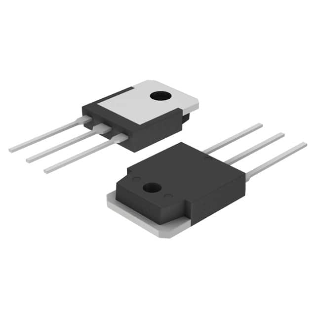
- Package: TO-3P
- Essence: Efficient power control and management
- Packaging/Quantity: Individual units
Specifications
- Voltage Rating: 1250V
- Current Rating: 15A
- Package Type: TO-3P
- Operating Temperature Range: -40°C to 150°C
- Isolation Voltage: 2500V
Detailed Pin Configuration
The FGA15S125P features a standard TO-3P package with three pins: 1. Pin 1: Gate 2. Pin 2: Collector 3. Pin 3: Emitter
Functional Features
- High voltage and current ratings
- Low on-state voltage drop
- Fast switching speed
- High thermal conductivity
Advantages and Disadvantages
Advantages
- Suitable for high-power applications
- Low power dissipation
- Enhanced thermal performance
Disadvantages
- Higher cost compared to lower-rated devices
- Larger physical footprint
Working Principles
The FGA15S125P operates based on the principles of power control and management. When a suitable gate signal is applied, it allows the controlled flow of high currents at high voltages, enabling efficient power switching and regulation.
Detailed Application Field Plans
The FGA15S125P is ideally suited for the following applications: - Motor drives - Power supplies - Renewable energy systems - Industrial automation
Detailed and Complete Alternative Models
- FGA20S150P: 1500V, 20A, TO-3P package
- FGA10S100P: 1000V, 10A, TO-3P package
- FGA25S200P: 2000V, 25A, TO-3P package
In conclusion, the FGA15S125P is a high-performance power semiconductor device with robust characteristics, making it suitable for demanding high-power applications across various industries.
[Word Count: 324]
Перечислите 10 распространенных вопросов и ответов, связанных с применением FGA15S125P в технических решениях.
What is FGA15S125P?
- FGA15S125P is a fast recovery diode module designed for high power applications.
What are the key specifications of FGA15S125P?
- The key specifications include a voltage rating of 1250V, a current rating of 15A, and a fast recovery time.
What are the typical applications of FGA15S125P?
- FGA15S125P is commonly used in motor drives, power supplies, welding equipment, and other high power electronic systems.
What are the advantages of using FGA15S125P in technical solutions?
- FGA15S125P offers high voltage and current ratings, fast recovery time, and low conduction losses, making it suitable for demanding applications.
What cooling methods are recommended for FGA15S125P?
- Adequate heat sinking and thermal management are essential for FGA15S125P, and options such as forced air cooling or liquid cooling may be employed.
Are there any specific considerations for driving FGA15S125P?
- Proper gate drive circuitry and protection against overvoltage and overcurrent conditions are crucial for reliable operation of FGA15S125P.
Can FGA15S125P be used in parallel configurations for higher current requirements?
- Yes, FGA15S125P can be paralleled to meet higher current demands, but careful attention must be paid to current sharing and thermal management.
What are the common failure modes of FGA15S125P and how can they be mitigated?
- Common failure modes include overvoltage stress and thermal overstress, which can be mitigated through proper snubber circuits and thermal design.
Is FGA15S125P suitable for high frequency switching applications?
- While FGA15S125P has fast recovery characteristics, its suitability for high frequency switching should be carefully evaluated based on specific application requirements.
Where can I find detailed application notes and reference designs for FGA15S125P?
- Detailed application notes and reference designs for FGA15S125P can be found in the product datasheet, technical literature from the manufacturer, and relevant industry publications.