

Подробную информацию о продукте см. в характеристиках.
NC7WV14P6X
Product Overview
- Category: Integrated Circuit (IC)
- Use: Logic Gate
- Characteristics: Low Voltage, High-Speed, Tiny Package
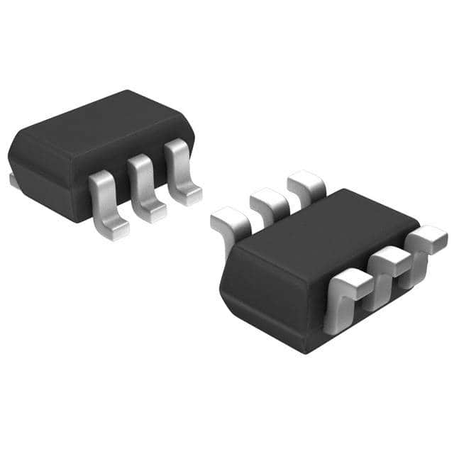
- Package: SOT-363
- Essence: Inverter Gate
- Packaging/Quantity: Tape and Reel, 3000 units per reel
Specifications
- Supply Voltage: 1.65V to 5.5V
- Input Voltage: 0V to VCC
- Output Voltage: 0V to VCC
- Propagation Delay: 2.5ns (typical)
- Operating Temperature Range: -40°C to +85°C
Detailed Pin Configuration
The NC7WV14P6X has a total of six pins:
- GND: Ground pin
- A: Input pin for the inverter gate
- Y: Output pin for the inverter gate
- NC: No Connection pin
- B: Input pin for the inverter gate
- VCC: Power supply pin
Functional Features
- Inverter Gate: The NC7WV14P6X is a single inverter gate that provides logic inversion of the input signal.
- Low Voltage Operation: It operates at a low voltage range of 1.65V to 5.5V, making it suitable for battery-powered devices.
- High-Speed Performance: With a propagation delay of only 2.5ns, it ensures fast signal processing.
- Tiny Package: The SOT-363 package offers a compact size, saving valuable board space.
Advantages and Disadvantages
Advantages
- Low voltage operation extends battery life in portable devices.
- High-speed performance enables quick signal processing.
- Tiny package saves board space in compact designs.
Disadvantages
- Limited number of gates per IC compared to larger packages.
- Sensitive to electrostatic discharge (ESD) due to small size.
Working Principles
The NC7WV14P6X operates based on the principles of CMOS (Complementary Metal-Oxide-Semiconductor) technology. It utilizes a combination of NMOS and PMOS transistors to achieve logic inversion. When the input signal is low, the NMOS transistor conducts, allowing current to flow from VCC to ground. This results in a high output voltage. Conversely, when the input signal is high, the PMOS transistor conducts, creating a low output voltage.
Detailed Application Field Plans
The NC7WV14P6X finds applications in various fields, including:
- Mobile Devices: It can be used in smartphones, tablets, and wearable devices for signal processing and level shifting.
- Consumer Electronics: It is suitable for use in digital cameras, portable media players, and gaming consoles for logic inversion and voltage translation.
- Automotive: The IC can be employed in automotive electronics for control systems, sensor interfacing, and communication modules.
- Industrial Automation: It finds utility in industrial automation equipment, such as PLCs (Programmable Logic Controllers), for logic operations and signal conditioning.
Detailed and Complete Alternative Models
- 74LVC1G04: Single Inverter Gate, 1.65V to 5.5V supply voltage range, SOT-353 package.
- SN74LVC1G04: Single Inverter Gate, 1.65V to 5.5V supply voltage range, SOT-23 package.
- NC7SZ14: Single Schmitt Trigger Inverter, 1.65V to 5.5V supply voltage range, SOT-353 package.
(Note: The above list is not exhaustive and serves as an example of alternative models.)
In conclusion, the NC7WV14P6X is a low-voltage, high-speed inverter gate IC that offers compact packaging and finds applications in various fields. Its advantages include low power consumption, fast signal processing, and space-saving design. However, it has limitations regarding the number of gates per IC and susceptibility to ESD. Alternative models with similar functionality are also available in the market.
Перечислите 10 распространенных вопросов и ответов, связанных с применением NC7WV14P6X в технических решениях.
Sure! Here are 10 common questions and answers related to the application of NC7WV14P6X in technical solutions:
Q: What is NC7WV14P6X? A: NC7WV14P6X is a specific type of integrated circuit (IC) or chip, commonly known as a hex inverter with Schmitt-trigger inputs.
Q: What is the purpose of NC7WV14P6X in technical solutions? A: NC7WV14P6X is used to convert digital signals, specifically inverters, and it incorporates Schmitt-trigger inputs for improved noise immunity.
Q: What voltage levels does NC7WV14P6X support? A: NC7WV14P6X supports a wide range of voltage levels, typically from 1.65V to 5.5V, making it compatible with various digital systems.
Q: Can NC7WV14P6X be used in battery-powered devices? A: Yes, NC7WV14P6X can be used in battery-powered devices as it operates at low power consumption and supports a wide voltage range.
Q: How many inverters are there in NC7WV14P6X? A: NC7WV14P6X contains six inverters, making it suitable for applications that require multiple signal conversions.
Q: What is the maximum operating frequency of NC7WV14P6X? A: The maximum operating frequency of NC7WV14P6X is typically around 50 MHz, which makes it suitable for most digital applications.
Q: Is NC7WV14P6X compatible with other logic families? A: Yes, NC7WV14P6X is compatible with various logic families, including TTL, CMOS, and LVCMOS, making it versatile for integration into different systems.
Q: Can NC7WV14P6X be used in high-speed data transmission applications? A: While NC7WV14P6X can handle moderate frequencies, it may not be suitable for high-speed data transmission applications that require very fast switching times.
Q: What are the typical package options available for NC7WV14P6X? A: NC7WV14P6X is commonly available in small surface-mount packages like SOT-23 and SC-70, which are suitable for compact designs.
Q: Are there any specific design considerations when using NC7WV14P6X? A: It is important to consider power supply decoupling, signal integrity, and noise immunity when designing with NC7WV14P6X to ensure optimal performance.
Please note that the answers provided here are general and may vary depending on specific datasheet specifications and application requirements.