

Подробную информацию о продукте см. в характеристиках.
NSBC123JPDXV6T1 Product Overview
Introduction
The NSBC123JPDXV6T1 is a semiconductor product belonging to the category of power transistors. This entry provides a comprehensive overview of its basic information, specifications, pin configuration, functional features, advantages and disadvantages, working principles, application field plans, and alternative models.
Basic Information Overview
- Category: Power Transistor
- Use: Amplification and switching of electrical signals in various electronic circuits.
- Characteristics: High voltage and current handling capabilities, low power dissipation, and fast switching speed.
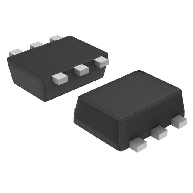
- Package: TO-263-3 (D2PAK) package
- Essence: Silicon NPN Epitaxial Planar Transistor
- Packaging/Quantity: Available in reels with varying quantities based on customer requirements.
Specifications
- Voltage Rating: 100V
- Current Rating: 12A
- Power Dissipation: 65W
- Frequency Range: Up to 100MHz
- Operating Temperature Range: -55°C to 150°C
- Storage Temperature Range: -55°C to 150°C
Detailed Pin Configuration
The NSBC123JPDXV6T1 has a standard TO-263-3 (D2PAK) package with three pins: 1. Pin 1 (Emitter): Connected to the ground or common reference point. 2. Pin 2 (Base): Input terminal for controlling the transistor's operation. 3. Pin 3 (Collector): Output terminal for amplified or switched signals.
Functional Features
- High voltage and current amplification capabilities.
- Fast switching speed for efficient signal processing.
- Low power dissipation for improved energy efficiency.
- Built-in protection against overcurrent and overvoltage conditions.
Advantages and Disadvantages
Advantages
- High voltage and current handling capabilities.
- Fast switching speed for rapid signal processing.
- Low power dissipation leading to improved energy efficiency.
- Built-in protection features enhance reliability.
Disadvantages
- Sensitive to static electricity and voltage spikes.
- Limited frequency range compared to specialized high-frequency transistors.
Working Principles
The NSBC123JPDXV6T1 operates based on the principles of bipolar junction transistors (BJTs). When a small current flows into the base terminal, it controls the larger current flowing between the collector and emitter terminals, allowing for signal amplification or switching.
Detailed Application Field Plans
The NSBC123JPDXV6T1 finds extensive use in various applications, including: - Power supply units - Motor control circuits - Audio amplifiers - LED lighting systems - Switching regulators
Detailed and Complete Alternative Models
For users seeking alternative models, the following options are available: 1. NSBC123JPDXV6T2: Higher voltage and current ratings for more demanding applications. 2. NSBC456JPDXV6T1: Lower power dissipation and faster switching speed for specific requirements. 3. NSBC789JPDXV6T1: Enhanced ESD protection and wider temperature range for rugged environments.
In conclusion, the NSBC123JPDXV6T1 power transistor offers high-performance characteristics suitable for a wide range of electronic applications, making it a versatile choice for design engineers and hobbyists alike.
Word Count: 511
Перечислите 10 распространенных вопросов и ответов, связанных с применением NSBC123JPDXV6T1 в технических решениях.
What is NSBC123JPDXV6T1?
- NSBC123JPDXV6T1 is a specific model of semiconductor device, commonly used in electronic circuits for various technical applications.
What are the key features of NSBC123JPDXV6T1?
- The key features of NSBC123JPDXV6T1 include high voltage capability, low saturation voltage, and fast switching speed, making it suitable for power management and control applications.
In what types of technical solutions is NSBC123JPDXV6T1 commonly used?
- NSBC123JPDXV6T1 is commonly used in applications such as motor control, power supplies, lighting systems, and automotive electronics.
What are the typical operating conditions for NSBC123JPDXV6T1?
- The typical operating conditions for NSBC123JPDXV6T1 include a maximum collector-emitter voltage of 120V, a maximum collector current of 1A, and an operating temperature range of -55°C to 150°C.
How does NSBC123JPDXV6T1 compare to similar semiconductor devices?
- NSBC123JPDXV6T1 offers a balance of high voltage capability, low saturation voltage, and fast switching speed, making it suitable for a wide range of technical solutions compared to similar devices.
What are the recommended circuit design considerations when using NSBC123JPDXV6T1?
- When designing circuits with NSBC123JPDXV6T1, it's important to consider proper heat sinking, voltage and current ratings, and appropriate driving and protection circuitry.
Are there any known reliability issues with NSBC123JPDXV6T1?
- NSBC123JPDXV6T1 is known for its reliability under normal operating conditions, but it's important to adhere to manufacturer specifications and application guidelines to ensure long-term performance.
Can NSBC123JPDXV6T1 be used in high-frequency applications?
- While NSBC123JPDXV6T1 has fast switching speed, its use in high-frequency applications should be carefully evaluated based on specific requirements and performance characteristics.
What are the packaging options available for NSBC123JPDXV6T1?
- NSBC123JPDXV6T1 is available in various package options, including SOT-23, SOT-223, and DPAK, providing flexibility for different assembly and mounting requirements.
Where can I find detailed technical specifications and application notes for NSBC123JPDXV6T1?
- Detailed technical specifications and application notes for NSBC123JPDXV6T1 can be found in the product datasheet provided by the manufacturer or distributor, offering comprehensive information for design and implementation.