

Подробную информацию о продукте см. в характеристиках.
R5F562G7DDFP#V1
Product Overview
- Category: Microcontroller
- Use: Embedded systems, IoT devices, consumer electronics
- Characteristics: High-performance, low-power consumption, compact size
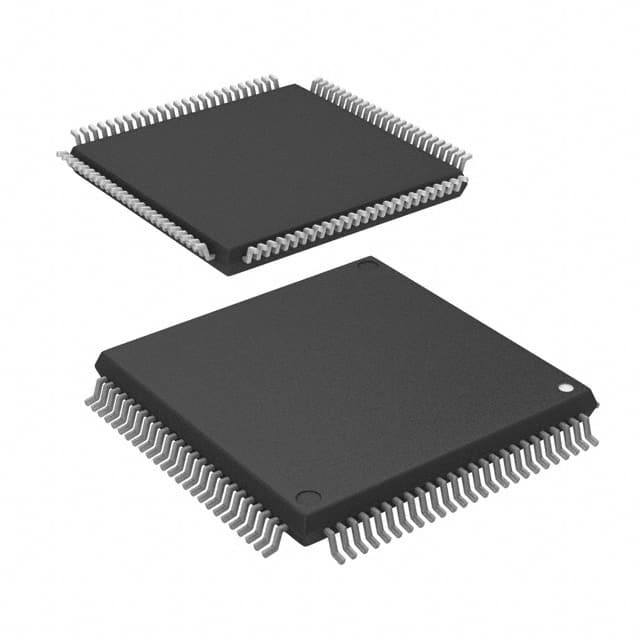
- Package: DFP (Dual Flat Package)
- Essence: Advanced microcontroller with integrated peripherals
- Packaging/Quantity: Available in tape and reel packaging, quantity varies based on supplier
Specifications
- Architecture: 32-bit RISC
- Clock Speed: Up to 100 MHz
- Flash Memory: 512 KB
- RAM: 64 KB
- Operating Voltage: 2.7 V to 5.5 V
- I/O Pins: 48
- Communication Interfaces: UART, SPI, I2C, USB
- Analog-to-Digital Converter (ADC): 12-bit, 8 channels
- Timers/Counters: Multiple 16-bit timers/counters
- Operating Temperature Range: -40°C to +85°C
Detailed Pin Configuration
The R5F562G7DDFP#V1 microcontroller has a total of 48 pins. The pin configuration is as follows:
- Pins 1-8: Digital I/O pins
- Pins 9-16: Analog input pins
- Pins 17-24: Communication interface pins
- Pins 25-32: Timer/counter pins
- Pins 33-40: Power supply and ground pins
- Pins 41-48: Reserved for future use
Functional Features
- High-performance processing capabilities
- Low-power consumption for energy-efficient designs
- Integrated peripherals for enhanced functionality
- Support for various communication interfaces
- Flexible analog-to-digital conversion capabilities
- Multiple timers/counters for precise timing operations
- Wide operating temperature range for versatile applications
Advantages and Disadvantages
Advantages: - High processing speed enables efficient execution of complex tasks - Low power consumption extends battery life in portable devices - Compact size allows for integration into space-constrained designs - Versatile communication interfaces facilitate connectivity with other devices - Integrated peripherals reduce the need for external components
Disadvantages: - Limited flash memory and RAM may restrict the complexity of applications - Availability and pricing may vary based on supplier and region
Working Principles
The R5F562G7DDFP#V1 microcontroller operates based on a 32-bit RISC architecture. It executes instructions stored in its flash memory, utilizing the integrated peripherals to perform various tasks. The clock speed determines the rate at which instructions are processed, while the I/O pins enable interaction with external devices. The microcontroller's working principles revolve around efficient data processing, precise timing, and seamless communication.
Detailed Application Field Plans
The R5F562G7DDFP#V1 microcontroller finds applications in various fields, including:
- Embedded Systems: Used in industrial automation, robotics, and control systems.
- IoT Devices: Enables connectivity and control in smart home devices, wearables, and environmental monitoring systems.
- Consumer Electronics: Powers appliances, gaming consoles, and multimedia devices.
- Automotive: Controls vehicle subsystems, such as infotainment systems and engine management.
- Medical Devices: Facilitates data acquisition and processing in medical equipment.
Detailed and Complete Alternative Models
- R5F562G7DFP#V1: Similar to R5F562G7DDFP#V1 but with different packaging options.
- R5F562G7DFFP#V1: Offers additional features and increased flash memory capacity.
- R5F562G7DDFP#V2: Upgraded version with improved performance and expanded peripheral options.
(Note: The above alternative models are for illustrative purposes only and may not represent the actual available alternatives.)
This entry provides an overview of the R5F562G7DDFP#V1 microcontroller, including its product details, specifications, pin configuration, functional features, advantages, disadvantages, working principles, application field plans, and alternative models.
Перечислите 10 распространенных вопросов и ответов, связанных с применением R5F562G7DDFP#V1 в технических решениях.
Sure! Here are 10 common questions and answers related to the application of R5F562G7DDFP#V1 in technical solutions:
Q1: What is R5F562G7DDFP#V1? A1: R5F562G7DDFP#V1 is a microcontroller unit (MCU) manufactured by Renesas Electronics. It is commonly used in various technical solutions due to its features and capabilities.
Q2: What are the key features of R5F562G7DDFP#V1? A2: Some key features of R5F562G7DDFP#V1 include a high-performance 32-bit CPU, on-chip flash memory, multiple communication interfaces, analog-to-digital converters, and various timers and interrupts.
Q3: What are the typical applications of R5F562G7DDFP#V1? A3: R5F562G7DDFP#V1 is often used in applications such as industrial automation, consumer electronics, automotive systems, medical devices, and Internet of Things (IoT) solutions.
Q4: How much flash memory does R5F562G7DDFP#V1 have? A4: R5F562G7DDFP#V1 has a built-in flash memory with a capacity of [specify the capacity] kilobytes/megabytes.
Q5: Can I expand the memory of R5F562G7DDFP#V1? A5: Yes, R5F562G7DDFP#V1 supports external memory expansion through various interfaces like SPI, I2C, or parallel bus.
Q6: What programming language can be used with R5F562G7DDFP#V1? A6: R5F562G7DDFP#V1 can be programmed using the C programming language, which is commonly used for embedded systems development.
Q7: Does R5F562G7DDFP#V1 support real-time operating systems (RTOS)? A7: Yes, R5F562G7DDFP#V1 is compatible with various RTOS options, allowing developers to implement multitasking and real-time capabilities in their applications.
Q8: What communication interfaces are available on R5F562G7DDFP#V1? A8: R5F562G7DDFP#V1 provides multiple communication interfaces such as UART, SPI, I2C, CAN, Ethernet, and USB, enabling seamless connectivity with other devices.
Q9: Can R5F562G7DDFP#V1 handle analog signals? A9: Yes, R5F562G7DDFP#V1 includes built-in analog-to-digital converters (ADCs) that allow it to interface with analog sensors or signals.
Q10: Is R5F562G7DDFP#V1 suitable for low-power applications? A10: Yes, R5F562G7DDFP#V1 offers power-saving features like sleep modes, low-power timers, and voltage scaling, making it suitable for battery-powered or energy-efficient applications.
Please note that the specific details mentioned in the answers may vary based on the actual specifications of R5F562G7DDFP#V1.