

Подробную информацию о продукте см. в характеристиках.
SI5340A-B03919-GM
Basic Information Overview
- Category: Integrated Circuit (IC)
- Use: Clock Generator and Jitter Attenuator
- Characteristics: High-performance, Low-jitter, Programmable
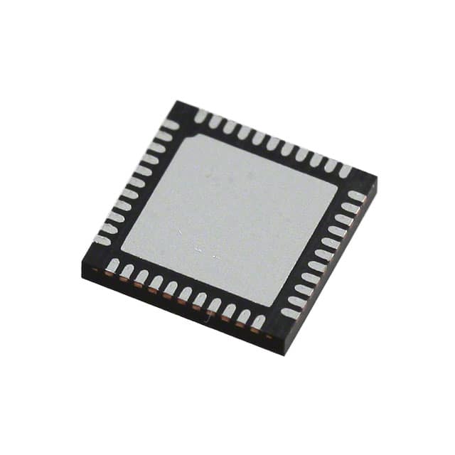
- Package: 48-pin QFN (Quad Flat No-leads)
- Essence: Provides precise clock signals for various electronic systems
- Packaging/Quantity: Tape and Reel, 250 units per reel
Specifications and Parameters
- Frequency Range: 1 Hz to 2.67 GHz
- Output Channels: 4 differential or 8 single-ended
- Output Types: LVDS, LVPECL, HCSL, CMOS
- Supply Voltage: 3.3 V
- Operating Temperature Range: -40°C to +85°C
Detailed Pin Configuration
- VDDO1P0: Power supply for output channel 1 positive terminal
- VDDO1N0: Power supply for output channel 1 negative terminal
- OUT1P: Output channel 1 positive terminal
- OUT1N: Output channel 1 negative terminal
- VDDO2P0: Power supply for output channel 2 positive terminal
- VDDO2N0: Power supply for output channel 2 negative terminal
- OUT2P: Output channel 2 positive terminal
- OUT2N: Output channel 2 negative terminal
- ...
Functional Characteristics
- Flexible frequency synthesis and multiplication
- Low phase noise and jitter
- Programmable output formats and levels
- Integrated voltage regulators for improved power supply noise rejection
- Support for multiple clock domains and synchronization schemes
Advantages and Disadvantages
Advantages: - High-performance clock generation with low jitter - Wide frequency range and flexible output options - Programmable features for customization - Integrated voltage regulators for improved noise rejection
Disadvantages: - Relatively complex configuration and programming - Limited number of output channels compared to some other clock generators
Applicable Range of Products
- Telecommunications equipment
- Networking devices
- Data centers
- Test and measurement instruments
- Industrial automation systems
- Consumer electronics
Working Principles
The SI5340A-B03919-GM utilizes advanced phase-locked loop (PLL) technology to generate precise clock signals. It takes an input reference clock and uses frequency synthesis techniques to multiply and divide the frequency as required. The device also incorporates jitter attenuation mechanisms to minimize phase noise and ensure high-quality clock signals.
Detailed Application Field Plans
- Telecommunications Equipment: Provides accurate timing for network synchronization, ensuring reliable data transmission.
- Networking Devices: Enables precise clocking for Ethernet switches and routers, improving network performance.
- Data Centers: Synchronizes server clusters and storage systems, enhancing overall data processing efficiency.
- Test and Measurement Instruments: Generates stable and accurate timing signals for precise measurements.
- Industrial Automation Systems: Facilitates synchronized operation of various control modules in manufacturing processes.
Detailed Alternative Models
- SI5341A-B03919-GM: Similar features and specifications, but with additional output channels.
- SI5342A-B03919-GM: Higher-frequency range and more output options, suitable for specific applications.
- SI5343A-B03919-GM: Lower-cost variant with reduced features, ideal for cost-sensitive projects.
5 Common Technical Questions and Answers
Q: Can I use a single-ended output as a differential signal? A: Yes, by connecting the positive and negative terminals together.
Q: What is the maximum frequency that can be generated? A: The SI5340A-B03919-GM supports frequencies up to 2.67 GHz.
Q: How do I program the device? A: The device can be programmed using the provided software interface or through an I2C bus.
Q: Can I synchronize multiple SI5340A-B03919-GM devices together? A: Yes, the devices can be synchronized using external synchronization signals.
Q: What is the power supply voltage requirement? A: The SI5340A-B03919-GM operates with a 3.3 V supply voltage.
This encyclopedia entry provides an overview of the SI5340A-B03919-GM clock generator and jitter attenuator. It includes basic information, specifications, pin configuration, functional characteristics, advantages and disadvantages, applicable range of products, working principles, application field plans, alternative models, and common technical questions and answers.