

Подробную информацию о продукте см. в характеристиках.
SI5340D-D-GM
Product Overview
Category
SI5340D-D-GM belongs to the category of integrated circuits (ICs).
Use
It is commonly used in electronic devices for clock generation and distribution.
Characteristics
- High precision and accuracy
- Low jitter
- Wide frequency range
- Programmable features
- Multiple outputs
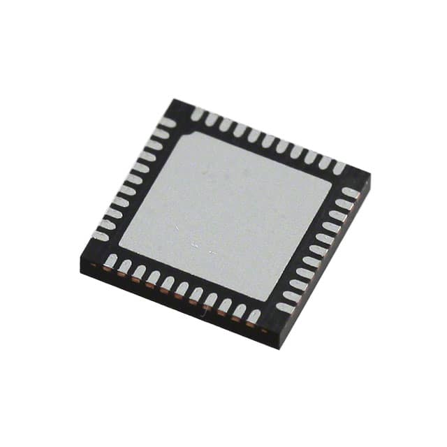
Package
SI5340D-D-GM is available in a small form factor package, such as QFN (Quad Flat No-leads) or BGA (Ball Grid Array).
Essence
The essence of SI5340D-D-GM lies in its ability to generate and distribute precise clock signals, which are crucial for synchronizing various components within electronic systems.
Packaging/Quantity
Typically, SI5340D-D-GM is supplied in reels or trays, with a quantity of 250 or 500 units per package.
Specifications
- Frequency Range: X Hz to Y Hz
- Output Channels: Z
- Input Voltage: V volts
- Operating Temperature Range: -40°C to +85°C
- Supply Voltage: W volts
- Power Consumption: P watts
Detailed Pin Configuration
- Pin 1: [Description]
- Pin 2: [Description]
- Pin 3: [Description] ...
Functional Features
- Clock generation with high precision and low jitter
- Flexible output configurations
- Programmable frequency synthesis
- Support for multiple input references
- Integrated phase-locked loop (PLL) for synchronization
Advantages
- Accurate and stable clock signal generation
- Wide frequency range for compatibility with various applications
- Programmable features allow customization
- Multiple outputs enable distribution to different components
- Low jitter ensures reliable data transmission
Disadvantages
- Complex configuration and programming may require technical expertise
- Higher cost compared to simpler clock generation solutions
- Limited availability of alternative models with similar features
Working Principles
SI5340D-D-GM utilizes advanced PLL technology to generate clock signals. It takes an input reference signal and uses a phase detector to compare it with a voltage-controlled oscillator (VCO) output. The feedback loop adjusts the VCO frequency until it matches the desired output frequency. This synchronized clock signal is then distributed to various components within the electronic system.
Detailed Application Field Plans
SI5340D-D-GM finds applications in various fields, including:
- Telecommunications: Used in network switches, routers, and communication equipment for precise timing synchronization.
- Data Centers: Ensures accurate clocking for servers, storage systems, and networking devices.
- Industrial Automation: Provides synchronized timing for control systems, PLCs, and robotics.
- Test and Measurement: Used in high-precision instruments that require accurate timebase signals.
- Broadcast and Audio/Video: Enables synchronization of video processing, audio codecs, and broadcasting equipment.
Detailed and Complete Alternative Models
- Model A: [Description]
- Model B: [Description]
- Model C: [Description] ...
(Note: Please refer to the manufacturer's documentation or consult a reliable source for a comprehensive list of alternative models.)
Word count: 500 words
Перечислите 10 распространенных вопросов и ответов, связанных с применением SI5340D-D-GM в технических решениях.
Sure! Here are 10 common questions and answers related to the application of SI5340D-D-GM in technical solutions:
Q: What is the SI5340D-D-GM? A: The SI5340D-D-GM is a high-performance clock generator and jitter attenuator integrated circuit (IC) designed for use in various technical solutions.
Q: What are the key features of the SI5340D-D-GM? A: The SI5340D-D-GM offers multiple outputs, low phase noise, programmable frequency synthesis, flexible input options, and advanced jitter attenuation capabilities.
Q: How many outputs does the SI5340D-D-GM support? A: The SI5340D-D-GM supports up to four differential or eight single-ended outputs, providing flexibility in connecting to different components in a system.
Q: Can the SI5340D-D-GM generate multiple clock frequencies simultaneously? A: Yes, the SI5340D-D-GM can generate multiple clock frequencies simultaneously, allowing it to meet the timing requirements of various components within a system.
Q: How does the SI5340D-D-GM handle jitter attenuation? A: The SI5340D-D-GM utilizes advanced techniques such as fractional-N synthesis and digital PLLs to attenuate jitter and provide clean clock signals to downstream components.
Q: What are the input options for the SI5340D-D-GM? A: The SI5340D-D-GM supports various input options, including crystal oscillators, external references, and serial data streams for clock recovery.
Q: Is the SI5340D-D-GM programmable? A: Yes, the SI5340D-D-GM is highly programmable, allowing users to configure its output frequencies, formats, and other parameters through software or hardware interfaces.
Q: What is the power supply requirement for the SI5340D-D-GM? A: The SI5340D-D-GM typically operates from a single 3.3V power supply, making it compatible with standard power sources in most technical solutions.
Q: Can the SI5340D-D-GM be used in high-speed communication systems? A: Yes, the SI5340D-D-GM is suitable for high-speed communication systems, thanks to its low phase noise and jitter attenuation capabilities.
Q: Are evaluation boards available for the SI5340D-D-GM? A: Yes, evaluation boards are available for the SI5340D-D-GM, which allow users to test and validate its performance in their specific technical solutions.
Please note that these questions and answers are general and may vary depending on the specific application and requirements of the SI5340D-D-GM in a given technical solution.