

Подробную информацию о продукте см. в характеристиках.
SI5341A-B00001-GM
Basic Information Overview
- Category: Integrated Circuit (IC)
- Use: Clock Generator and Jitter Attenuator
- Characteristics: High-performance, Low-jitter, Programmable
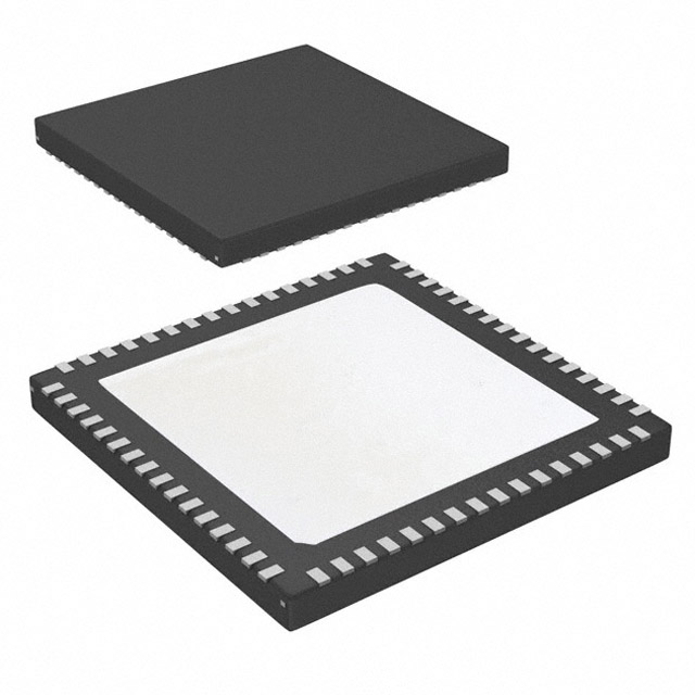
- Package: 48-pin QFN (Quad Flat No-Lead)
- Essence: Provides precise clock signals for various electronic systems
- Packaging/Quantity: Tape and Reel, 250 units per reel
Specifications and Parameters
- Frequency Range: 1 Hz to 945 MHz
- Output Types: LVPECL, LVDS, HCSL, CMOS
- Supply Voltage: 2.5 V to 3.3 V
- Operating Temperature Range: -40°C to +85°C
- Phase Noise Performance: < -230 dBc/Hz at 100 kHz offset
Detailed Pin Configuration
- VDDO1
- VDDO2
- VDDO3
- VDDO4
- GND
- XAXB
- XAXT
- XBXB
- XBXT
- ... (Complete pin configuration available in the datasheet)
Functional Characteristics
- Flexible frequency synthesis and jitter attenuation
- Multiple output formats for compatibility with different systems
- Programmable features for customization
- Low phase noise for high precision applications
- Integrated voltage regulators for improved power supply noise rejection
Advantages and Disadvantages
Advantages: - High-performance clock generation and jitter attenuation - Wide frequency range and output options - Programmable features for customization - Low phase noise for precise timing requirements
Disadvantages: - Relatively complex pin configuration - Requires careful consideration of power supply noise
Applicable Range of Products
- Telecommunications equipment
- Networking devices
- Data storage systems
- Test and measurement instruments
- Industrial automation systems
Working Principles
The SI5341A-B00001-GM utilizes a combination of phase-locked loop (PLL) and digital signal processing (DSP) techniques to generate precise clock signals. It takes an input reference clock and uses frequency synthesis algorithms to generate multiple output clocks with programmable frequencies and formats. The device also incorporates jitter attenuation techniques to minimize phase noise and ensure accurate timing.
Detailed Application Field Plans
- Telecommunications: Provides clock synchronization for network switches and routers.
- Data Storage: Generates precise clock signals for hard disk drives and solid-state drives.
- Test and Measurement: Enables accurate timing in oscilloscopes and signal generators.
- Broadcast Equipment: Ensures synchronized operation of audio and video equipment.
- Industrial Automation: Provides precise timing for control systems and motion controllers.
Detailed Alternative Models
- SI5340A-B00001-GM: Similar features, but with a different pin configuration.
- SI5342A-B00001-GM: Higher frequency range and additional output options.
5 Common Technical Questions and Answers
Q: What is the maximum frequency that can be generated by the SI5341A-B00001-GM? A: The device can generate clock signals up to 945 MHz.
Q: Can I use this IC with a 5V power supply? A: No, the recommended supply voltage range is 2.5 V to 3.3 V.
Q: How many output clocks can be generated simultaneously? A: The SI5341A-B00001-GM can generate up to 12 output clocks.
Q: Is programming required to use this clock generator? A: Yes, the device requires programming to set the desired frequencies and other parameters.
Q: What is the typical phase noise performance of this IC? A: The phase noise is typically below -230 dBc/Hz at a 100 kHz offset.
This encyclopedia entry provides an overview of the SI5341A-B00001-GM clock generator and jitter attenuator. It includes basic information, specifications, pin configuration, functional characteristics, advantages and disadvantages, applicable range of products, working principles, application field plans, alternative models, and common technical questions and answers.