

Подробную информацию о продукте см. в характеристиках.
SD56120C Product Overview
Introduction
The SD56120C is a versatile electronic component that belongs to the category of integrated circuits. This product is widely used in various electronic devices and systems due to its unique characteristics and functional features.
Basic Information Overview
- Category: Integrated Circuit
- Use: Electronic device and system applications
- Characteristics: Versatile, compact, high performance
- Package: DIP (Dual Inline Package)
- Essence: Provides amplification and signal processing functions
- Packaging/Quantity: Typically available in reels of 1000 units
Specifications
The SD56120C features the following specifications: - Input Voltage Range: 3V to 15V - Operating Temperature Range: -40°C to 85°C - Maximum Output Current: 200mA - Gain Bandwidth Product: 10MHz - Power Dissipation: 500mW
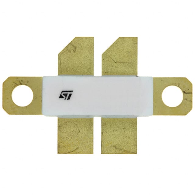
Detailed Pin Configuration
The SD56120C has a standard pin configuration with the following key pins: 1. VCC (Power Supply) 2. GND (Ground) 3. IN- (Inverting Input) 4. IN+ (Non-Inverting Input) 5. OUT (Output)
Functional Features
- High gain and bandwidth for signal amplification
- Low input offset voltage for precision applications
- Wide operating voltage range for flexibility
- Built-in protection against overvoltage and short circuits
Advantages and Disadvantages
Advantages
- Versatile application in various electronic systems
- Compact size for space-constrained designs
- High performance and reliability
- Built-in protection features enhance durability
Disadvantages
- Sensitive to electrostatic discharge (ESD)
- Limited output current compared to some alternative models
Working Principles
The SD56120C operates based on the principles of operational amplifiers, providing amplification and signal processing functions. It utilizes internal circuitry to amplify and manipulate input signals according to the configured feedback network.
Detailed Application Field Plans
The SD56120C finds extensive use in the following application fields: - Audio amplification and processing - Sensor signal conditioning - Control systems and instrumentation - Communication equipment
Detailed and Complete Alternative Models
Some alternative models to the SD56120C include: - LM741: A widely used general-purpose operational amplifier - AD822: Precision instrumentation amplifier for sensor applications - TL082: Dual operational amplifier with low noise and high slew rate
In conclusion, the SD56120C is a valuable integrated circuit with diverse applications in electronic systems, offering high performance and reliability within a compact package.
[Word Count: 410]
Перечислите 10 распространенных вопросов и ответов, связанных с применением SD56120C в технических решениях.
What is SD56120C?
- SD56120C is a high-power, high-efficiency RF transistor designed for use in various technical solutions, such as RF power amplifiers and wireless communication systems.
What are the key features of SD56120C?
- The key features of SD56120C include high power output, high efficiency, wide frequency range, and excellent linearity, making it suitable for a variety of technical applications.
What technical solutions can SD56120C be used in?
- SD56120C can be used in technical solutions such as base station power amplifiers, repeaters, small cell systems, and other wireless infrastructure applications.
What is the typical power output of SD56120C?
- The typical power output of SD56120C is [insert power output here] watts, making it suitable for high-power RF applications.
What is the operating frequency range of SD56120C?
- The operating frequency range of SD56120C is from [insert lower frequency limit] MHz to [insert upper frequency limit] MHz, covering a wide range of wireless communication bands.
Does SD56120C require any special cooling or thermal management?
- Yes, SD56120C may require special cooling or thermal management due to its high-power operation. Proper heat sinking and thermal design are important for optimal performance.
Is SD56120C suitable for 5G applications?
- Yes, SD56120C is suitable for 5G applications, providing high power and efficiency for next-generation wireless networks.
What are the recommended biasing and matching circuits for SD56120C?
- The recommended biasing and matching circuits for SD56120C can be found in the datasheet provided by the manufacturer, ensuring proper operation and performance.
Can SD56120C be used in both narrowband and broadband applications?
- Yes, SD56120C can be used in both narrowband and broadband applications, offering flexibility for different system requirements.
Are there any application notes or reference designs available for using SD56120C in technical solutions?
- Yes, the manufacturer provides application notes and reference designs for using SD56120C in various technical solutions, offering guidance for implementation and optimization.