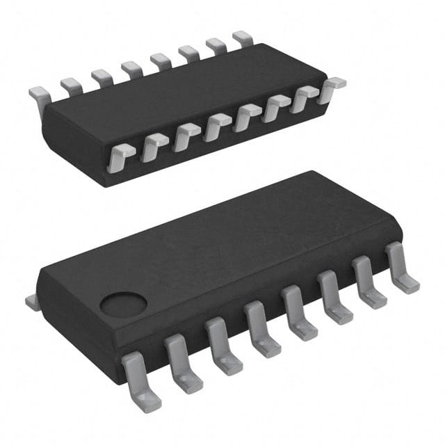
Подробную информацию о продукте см. в характеристиках.

CD4049UBDR
Product Overview
- Category: Integrated Circuit (IC)
- Use: Logic Inverter and Buffer
- Characteristics: High Voltage CMOS Hex Inverting Buffer/Converter
- Package: SOIC-16
- Essence: Hex Inverter with CMOS Technology
- Packaging/Quantity: Tape and Reel, 2500 pieces per reel
Specifications
The CD4049UBDR is a high voltage CMOS hex inverting buffer/converter integrated circuit. It operates on a wide voltage range from 3V to 18V, making it suitable for various applications. The IC has six independent inverters, each capable of converting logic level signals.
Key specifications include:
- Supply Voltage Range: 3V to 18V
- Input Voltage Range: 0V to VDD
- Output Voltage Range: 0V to VDD
- Maximum Input Current: ±1µA
- Maximum Quiescent Supply Current: 10µA
- Maximum Propagation Delay: 60ns
Pin Configuration
The CD4049UBDR has a total of 16 pins arranged in a SOIC-16 package. The pin configuration is as follows:
+---\/---+
   A1 -|1      16|- VDD
   A2 -|2      15|- Y6
   B1 -|3      14|- Y5
   B2 -|4      13|- Y4
   C1 -|5      12|- Y3
   C2 -|6      11|- Y2
   D1 -|7      10|- Y1
  GND -|8       9|- Y0
        +--------+
Functional Features
The CD4049UBDR offers the following functional features:
- High Voltage Operation: The IC can operate within a wide voltage range, making it suitable for various applications.
- Hex Inverting Buffer/Converter: It consists of six independent inverters that can convert logic level signals.
- CMOS Technology: The IC utilizes CMOS technology, providing low power consumption and high noise immunity.
- Wide Input Voltage Range: The CD4049UBDR accepts input voltages from 0V to VDD, allowing compatibility with different logic levels.
Advantages and Disadvantages
Advantages:
- Wide operating voltage range allows flexibility in different applications.
- Low power consumption due to CMOS technology.
- High noise immunity ensures reliable signal conversion.
- Compact SOIC-16 package enables space-saving designs.
Disadvantages:
- Limited output current capability.
- Propagation delay may affect timing-sensitive applications.
- Not suitable for high-speed applications due to slower switching speeds compared to other technologies.
Working Principles
The CD4049UBDR operates based on the principles of CMOS technology. Each inverter within the IC consists of complementary MOS transistors that control the flow of current between the input and output. When the input is high, the output becomes low, and vice versa.
The CMOS technology used in the CD4049UBDR provides low power consumption by minimizing static power dissipation. It also offers high noise immunity, making the IC less susceptible to external interference.
Application Field Plans
The CD4049UBDR finds applications in various fields, including:
- Digital Logic Circuits: It can be used as a logic inverter or buffer in digital systems.
- Signal Level Shifting: The IC can convert logic levels between different voltage domains.
- Sensor Interfaces: It can interface sensors with different logic levels to microcontrollers or other digital devices.
- Power Management: The CD4049UBDR can be utilized in power management circuits for voltage level conversion.
Alternative Models
There are several alternative models available that offer similar functionality to the CD4049UBDR. Some popular alternatives include:
- CD4069UB: Hex Inverter with CMOS Technology, DIP-14 package.
- 74HC04: Hex Inverter with High-Speed CMOS Technology, SOIC-14 package.
- SN74LS04: Hex Inverter with TTL Technology, DIP-14 package.
These alternative models can be considered based on specific requirements and compatibility with existing designs.
In conclusion, the CD4049UBDR is a high voltage CMOS hex inverting buffer/converter IC. It offers wide operating voltage range, low power consumption, and high noise immunity. With its compact package and versatile applications, it serves as a reliable component in digital logic circuits, signal level shifting, sensor interfaces, and power management systems.
Перечислите 10 распространенных вопросов и ответов, связанных с применением CD4049UBDR в технических решениях.
Sure! Here are 10 common questions and answers related to the application of CD4049UBDR:
Question: What is CD4049UBDR?
- Answer: CD4049UBDR is a hex inverter/buffer IC (integrated circuit) that can be used in various technical solutions.Question: What is the operating voltage range for CD4049UBDR?
- Answer: The operating voltage range for CD4049UBDR is typically between 3V and 18V.Question: Can CD4049UBDR be used as a level shifter?
- Answer: Yes, CD4049UBDR can be used as a level shifter to convert signals from one voltage level to another.Question: How many inverters are there in CD4049UBDR?
- Answer: CD4049UBDR has six inverters in a single package.Question: What is the maximum output current of CD4049UBDR?
- Answer: The maximum output current of CD4049UBDR is typically around 6mA.Question: Can CD4049UBDR be used in high-speed applications?
- Answer: CD4049UBDR is not specifically designed for high-speed applications, but it can be used in moderate-speed digital circuits.Question: Is CD4049UBDR compatible with TTL (Transistor-Transistor Logic) inputs?
- Answer: Yes, CD4049UBDR is compatible with TTL inputs and can be used as a drop-in replacement for TTL inverters.Question: Can CD4049UBDR be used in analog applications?
- Answer: CD4049UBDR is primarily designed for digital applications, but it can be used in some simple analog applications as well.Question: What is the typical power consumption of CD4049UBDR?
- Answer: The typical power consumption of CD4049UBDR is low, making it suitable for battery-powered applications.Question: Can CD4049UBDR be used in automotive applications?
- Answer: Yes, CD4049UBDR can be used in automotive applications as long as the operating voltage range and temperature requirements are met.
Please note that these answers are general and may vary depending on specific application requirements and datasheet specifications.

