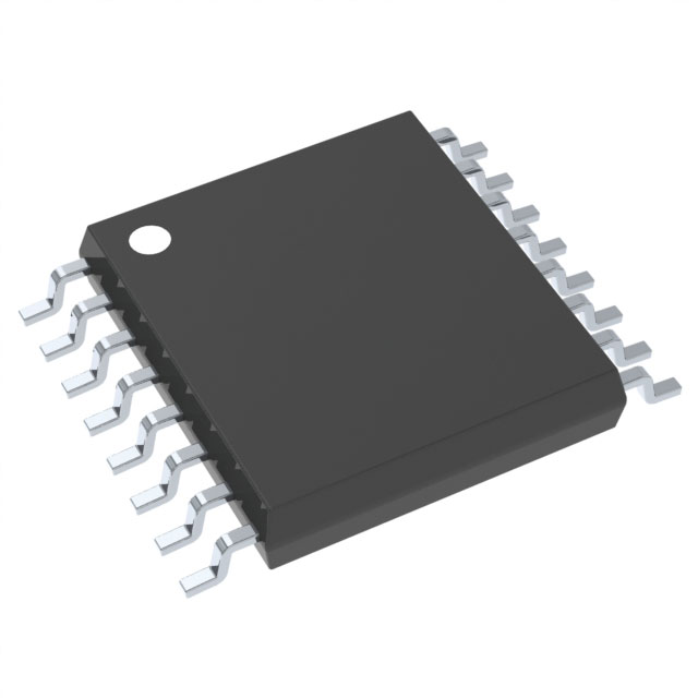
Подробную информацию о продукте см. в характеристиках.

CD74HC112PW
Product Overview
- Category: Integrated Circuit
- Use: Logic Gate
- Characteristics: High-Speed, Dual J-K Flip-Flop
- Package: TSSOP (Thin Shrink Small Outline Package)
- Essence: The CD74HC112PW is a dual J-K flip-flop integrated circuit that operates at high speed and is commonly used in digital logic applications.
- Packaging/Quantity: Available in reels of 2500 units.
Specifications
- Supply Voltage: 2V to 6V
- Logic Family: HC
- Number of Flip-Flops: 2
- Clock Trigger Type: Positive Edge-Triggered
- Output Type: Complementary
- Propagation Delay: 14 ns (typical)
- Operating Temperature Range: -40°C to +85°C
Detailed Pin Configuration
The CD74HC112PW has a total of 16 pins. The pin configuration is as follows:
- CLR (Clear Input for both flip-flops)
- CLK (Clock Input)
- J1 (J Input for the first flip-flop)
- K1 (K Input for the first flip-flop)
- Q1 (Output Q for the first flip-flop)
- Q̅1 (Complementary Output Q̅ for the first flip-flop)
- GND (Ground)
- Q̅2 (Complementary Output Q̅ for the second flip-flop)
- Q2 (Output Q for the second flip-flop)
- K2 (K Input for the second flip-flop)
- J2 (J Input for the second flip-flop)
- VCC (Positive Power Supply)
Functional Features
- Dual J-K flip-flop with independent clock inputs and clear inputs.
- Positive edge-triggered operation allows synchronous control of the flip-flops.
- Complementary outputs provide both true and inverted outputs.
- High-speed operation makes it suitable for time-critical applications.
- Wide operating voltage range allows flexibility in power supply selection.
Advantages and Disadvantages
Advantages: - Dual flip-flop design provides versatility in circuit design. - High-speed operation enables efficient data processing. - Clear inputs allow for easy initialization of the flip-flops. - Complementary outputs facilitate logical operations.
Disadvantages: - Limited number of flip-flops may restrict complex circuit implementation. - Requires external components for proper functioning. - Sensitivity to voltage fluctuations may affect performance.
Working Principles
The CD74HC112PW is a dual J-K flip-flop that operates based on positive edge-triggered clock inputs. Each flip-flop has independent J and K inputs, allowing for individual control. The clear input (CLR) resets both flip-flops to a known state when activated. The complementary outputs (Q and Q̅) provide both true and inverted outputs, enabling various logical operations.
Detailed Application Field Plans
The CD74HC112PW finds applications in various digital logic circuits, including but not limited to: - Counters and frequency dividers - Shift registers - Data storage and retrieval systems - Synchronous sequential circuits - Control systems
Detailed and Complete Alternative Models
Some alternative models to the CD74HC112PW include: - SN74HC112N by Texas Instruments - MC74HC112AN by ON Semiconductor - 74HC112 by NXP Semiconductors - CD4013B by Texas Instruments
These alternative models offer similar functionality and can be used as replacements depending on specific requirements.
Word count: 410 words
Перечислите 10 распространенных вопросов и ответов, связанных с применением CD74HC112PW в технических решениях.
Sure! Here are 10 common questions and answers related to the application of CD74HC112PW in technical solutions:
Q: What is CD74HC112PW? A: CD74HC112PW is a dual J-K flip-flop integrated circuit (IC) that can be used in various digital logic applications.
Q: What is the operating voltage range for CD74HC112PW? A: CD74HC112PW operates within a voltage range of 2V to 6V.
Q: What is the maximum clock frequency supported by CD74HC112PW? A: CD74HC112PW supports a maximum clock frequency of 25 MHz.
Q: Can CD74HC112PW be used in both synchronous and asynchronous applications? A: Yes, CD74HC112PW can be used in both synchronous and asynchronous applications.
Q: How many flip-flops are there in CD74HC112PW? A: CD74HC112PW contains two independent J-K flip-flops.
Q: What is the typical propagation delay of CD74HC112PW? A: The typical propagation delay of CD74HC112PW is around 15 ns.
Q: Does CD74HC112PW have any built-in preset or clear functionality? A: No, CD74HC112PW does not have any built-in preset or clear functionality.
Q: Can CD74HC112PW operate at high temperatures? A: CD74HC112PW has a wide operating temperature range of -40°C to +85°C, making it suitable for various environments.
Q: What is the package type of CD74HC112PW? A: CD74HC112PW is available in a standard 16-pin TSSOP (Thin Shrink Small Outline Package) package.
Q: What are some common applications of CD74HC112PW? A: CD74HC112PW is commonly used in counters, frequency dividers, shift registers, and other digital logic circuits where flip-flops are required.
Please note that the answers provided here are general and may vary depending on specific datasheet specifications and application requirements.

