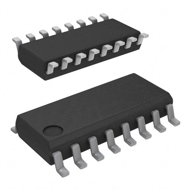
Подробную информацию о продукте см. в характеристиках.

CD74HC283MG4
Product Overview
Category
CD74HC283MG4 belongs to the category of integrated circuits (ICs).
Use
This product is commonly used in digital electronics and computer systems for arithmetic operations, specifically for performing high-speed binary addition.
Characteristics
- High-speed operation
- Low power consumption
- Wide operating voltage range
- Compatibility with various logic families
- Compact package size
Package
CD74HC283MG4 is available in a small outline integrated circuit (SOIC) package.
Essence
The essence of CD74HC283MG4 lies in its ability to perform fast and accurate binary addition, making it an essential component in many digital systems.
Packaging/Quantity
This product is typically packaged in reels or tubes, with each reel or tube containing a specific quantity of CD74HC283MG4 ICs.
Specifications
- Supply Voltage: 2V to 6V
- Logic Family: HC
- Number of Inputs: 8
- Number of Outputs: 4
- Operating Temperature Range: -40°C to +85°C
- Propagation Delay: 9 ns (typical)
Detailed Pin Configuration
CD74HC283MG4 has a total of 16 pins. The pin configuration is as follows:
- A1 (Input)
- B1 (Input)
- A0 (Input)
- B0 (Input)
- CIN (Input)
- S0 (Output)
- S1 (Output)
- S2 (Output)
- S3 (Output)
- GND (Ground)
- COUT (Output)
- LT (Output)
- LE (Input)
- CLK (Input)
- VCC (Power)
- B2 (Input)
Functional Features
CD74HC283MG4 offers the following functional features:
- High-speed binary addition
- Carry-in (CIN) and carry-out (COUT) functionality
- Enable/disable control (LE pin)
- Latch enable (LT) output for cascading multiple ICs
Advantages and Disadvantages
Advantages
- Fast operation allows for efficient arithmetic calculations
- Low power consumption helps in reducing overall system energy requirements
- Wide operating voltage range provides flexibility in various applications
- Compatibility with different logic families enables easy integration into existing systems
- Compact package size saves board space and simplifies circuit design
Disadvantages
- Limited number of inputs and outputs may restrict complex operations
- Propagation delay of 9 ns may introduce timing issues in certain high-speed applications
Working Principles
CD74HC283MG4 operates based on the principles of binary addition. It takes two 4-bit binary numbers (A and B) as inputs, along with a carry-in (CIN) signal. The IC performs the addition operation and generates a 4-bit sum (S0-S3) and a carry-out (COUT) signal. The LE pin can be used to enable or disable the IC's functionality, while the LT output facilitates cascading multiple ICs for larger bit-width additions.
Detailed Application Field Plans
CD74HC283MG4 finds extensive application in various fields, including:
- Digital calculators
- Microcontrollers
- Arithmetic logic units (ALUs)
- Data processing systems
- Communication devices
- Industrial automation
Detailed and Complete Alternative Models
Some alternative models that offer similar functionality to CD74HC283MG4 include:
- SN74HC283: This IC is from Texas Instruments and has comparable specifications.
- MC74HC283: Manufactured by ON Semiconductor, this IC is another suitable alternative.
- 74HCT283: This IC, available from multiple manufacturers, offers compatibility with TTL logic levels.
These alternative models can be considered based on specific project requirements and availability.
Word count: 523 words
Перечислите 10 распространенных вопросов и ответов, связанных с применением CD74HC283MG4 в технических решениях.
Sure! Here are 10 common questions and answers related to the application of CD74HC283MG4 in technical solutions:
Q: What is CD74HC283MG4? A: CD74HC283MG4 is a high-speed CMOS logic IC, specifically a 4-bit binary full adder with fast carry.
Q: What are the key features of CD74HC283MG4? A: Some key features include low power consumption, high-speed operation, wide operating voltage range, and compatibility with TTL inputs.
Q: How can CD74HC283MG4 be used in technical solutions? A: CD74HC283MG4 can be used for arithmetic operations, such as addition, subtraction, and multiplication, in digital circuits and microcontroller-based systems.
Q: What is the maximum operating frequency of CD74HC283MG4? A: The maximum operating frequency of CD74HC283MG4 is typically around 50 MHz.
Q: Can CD74HC283MG4 handle both positive and negative numbers? A: No, CD74HC283MG4 is designed to work with positive numbers only. It does not have built-in support for handling negative numbers.
Q: Does CD74HC283MG4 require external components for operation? A: Yes, CD74HC283MG4 requires external power supply connections and decoupling capacitors for stable operation.
Q: What is the power supply voltage range for CD74HC283MG4? A: CD74HC283MG4 operates within a power supply voltage range of 2V to 6V.
Q: Can CD74HC283MG4 be cascaded to perform operations on larger bit numbers? A: Yes, multiple CD74HC283MG4 ICs can be cascaded together to perform operations on larger bit numbers, such as 8-bit or 16-bit.
Q: Is CD74HC283MG4 suitable for battery-powered applications? A: Yes, CD74HC283MG4 is known for its low power consumption, making it suitable for battery-powered applications where power efficiency is crucial.
Q: Are there any alternative ICs to CD74HC283MG4 for similar applications? A: Yes, some alternative ICs include SN74LS283 and SN74HC283, which offer similar functionality but may have different specifications and performance characteristics.
Please note that the answers provided here are general in nature and may vary depending on specific datasheet information and application requirements.

