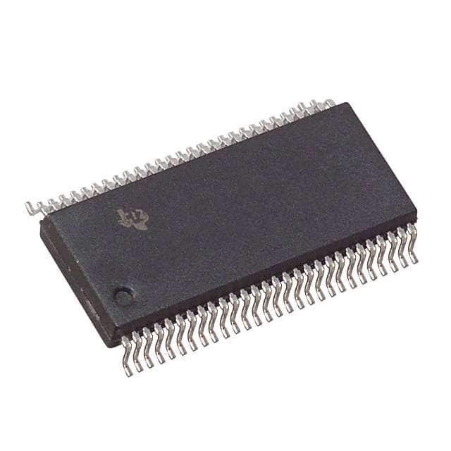
Подробную информацию о продукте см. в характеристиках.

SN74ABT162501DLR
Product Overview
- Category: Integrated Circuit (IC)
- Use: Data Buffer/Driver
- Characteristics: High-speed, non-inverting, 16-bit bus buffer with 3-state outputs
- Package: 56-pin TSSOP (Thin Shrink Small Outline Package)
- Essence: The SN74ABT162501DLR is designed to provide buffering and driving capabilities for a 16-bit bus. It allows bidirectional transfer of data between different voltage domains or systems.
- Packaging/Quantity: The SN74ABT162501DLR is typically sold in reels containing 250 units.
Specifications
- Supply Voltage: 4.5V to 5.5V
- Input Voltage Levels: 0V to VCC
- Output Voltage Levels: 0V to VCC
- Operating Temperature Range: -40°C to +85°C
- Propagation Delay: 2.8ns (typical)
- Output Drive Capability: ±24mA
Detailed Pin Configuration
The SN74ABT162501DLR has a total of 56 pins. Here is the detailed pin configuration:
- OE (Output Enable) 1
- Y1 (Output) 1
- GND (Ground)
- Y2 (Output) 1
- Y3 (Output) 1
- Y4 (Output) 1
- Y5 (Output) 1
- Y6 (Output) 1
- Y7 (Output) 1
- Y8 (Output) 1
- Y9 (Output) 1
- Y10 (Output) 1
- Y11 (Output) 1
- Y12 (Output) 1
- VCC (Supply Voltage)
- Y13 (Output) 1
- Y14 (Output) 1
- Y15 (Output) 1
- Y16 (Output) 1
- GND (Ground)
- A1 (Input) 1
- B1 (Input) 1
- A2 (Input) 1
- B2 (Input) 1
- A3 (Input) 1
- B3 (Input) 1
- A4 (Input) 1
- B4 (Input) 1
- A5 (Input) 1
- B5 (Input) 1
- A6 (Input) 1
- B6 (Input) 1
- A7 (Input) 1
- B7 (Input) 1
- A8 (Input) 1
- B8 (Input) 1
- GND (Ground)
- A9 (Input) 1
- B9 (Input) 1
- A10 (Input) 1
- B10 (Input) 1
- A11 (Input) 1
- B11 (Input) 1
- A12 (Input) 1
- B12 (Input) 1
- A13 (Input) 1
- B13 (Input) 1
- A14 (Input) 1
- B14 (Input) 1
- A15 (Input) 1
- B15 (Input) 1
- A16 (Input) 1
- B16 (Input) 1
- GND (Ground)
- OE (Output Enable) 2
- Y1 (Output) 2
Functional Features
- Bidirectional data transfer between different voltage domains or systems.
- Non-inverting buffer with 3-state outputs.
- High-speed operation for efficient data transfer.
- Output enable control for easy interfacing with other devices.
Advantages and Disadvantages
Advantages: - Allows bidirectional data transfer, enhancing system flexibility. - High-speed operation enables efficient data processing. - 3-state outputs provide control over the bus lines. - Wide operating temperature range allows usage in various environments.
Disadvantages: - Limited output drive capability may not be suitable for high-current applications. - Requires careful consideration of voltage compatibility between input and output systems.
Working Principles
The SN74ABT162501DLR operates by receiving input data on its A1-A16 and B1-B16 pins. The data is then buffered and driven to the corresponding Y1-Y16 output pins. The direction of data transfer is controlled by the OE (Output Enable)
Перечислите 10 распространенных вопросов и ответов, связанных с применением SN74ABT162501DLR в технических решениях.
Sure! Here are 10 common questions and answers related to the application of SN74ABT162501DLR in technical solutions:
Q: What is SN74ABT162501DLR? A: SN74ABT162501DLR is a 16-bit bus transceiver with 3-state outputs, designed for high-speed digital systems.
Q: What is the operating voltage range of SN74ABT162501DLR? A: The operating voltage range is typically between 4.5V and 5.5V.
Q: What is the maximum data transfer rate supported by SN74ABT162501DLR? A: SN74ABT162501DLR supports a maximum data transfer rate of 250 MHz.
Q: Can SN74ABT162501DLR be used for bidirectional data communication? A: Yes, SN74ABT162501DLR can be used for bidirectional data communication as it has separate input and output ports.
Q: How many bits can SN74ABT162501DLR handle at a time? A: SN74ABT162501DLR is a 16-bit bus transceiver, meaning it can handle 16 bits of data simultaneously.
Q: Does SN74ABT162501DLR support 3-state outputs? A: Yes, SN74ABT162501DLR supports 3-state outputs, allowing multiple devices to share a common bus without interference.
Q: What is the typical propagation delay of SN74ABT162501DLR? A: The typical propagation delay of SN74ABT162501DLR is around 3.8 ns.
Q: Can SN74ABT162501DLR be used in high-speed applications? A: Yes, SN74ABT162501DLR is designed for high-speed digital systems and can be used in high-speed applications.
Q: Does SN74ABT162501DLR have built-in ESD protection? A: Yes, SN74ABT162501DLR has built-in ESD protection to prevent damage from electrostatic discharge.
Q: What package does SN74ABT162501DLR come in? A: SN74ABT162501DLR is available in a 56-pin TSSOP (Thin Shrink Small Outline Package) package.
Please note that the answers provided here are general and may vary depending on specific datasheet specifications and application requirements.

