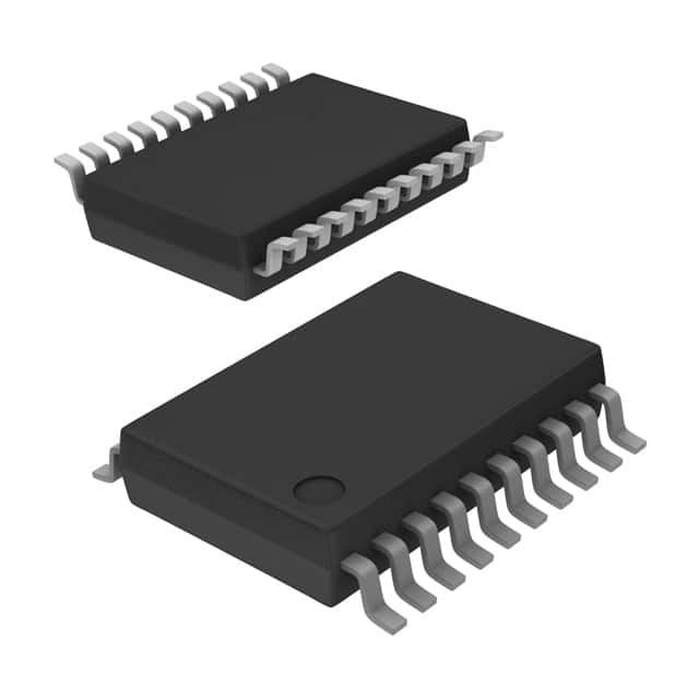
Подробную информацию о продукте см. в характеристиках.

SN74ABT273DBR
Product Overview
- Category: Integrated Circuit (IC)
- Use: Flip-Flop
- Characteristics: High-speed, low-power consumption
- Package: SSOP-20
- Essence: D-type flip-flop with reset
- Packaging/Quantity: Tape and Reel, 2500 pieces per reel
Specifications
- Supply Voltage Range: 4.5V to 5.5V
- Input Voltage Range: 0V to VCC
- Output Voltage Range: 0V to VCC
- Operating Temperature Range: -40°C to +85°C
- Propagation Delay Time: 3.8ns (typical)
- Output Current: ±24mA
Detailed Pin Configuration
The SN74ABT273DBR has a total of 20 pins. The pin configuration is as follows:
- CLR (Clear)
- D0 (Data Input 0)
- D1 (Data Input 1)
- D2 (Data Input 2)
- D3 (Data Input 3)
- D4 (Data Input 4)
- D5 (Data Input 5)
- D6 (Data Input 6)
- D7 (Data Input 7)
- GND (Ground)
- Q7 (Output 7)
- Q6 (Output 6)
- Q5 (Output 5)
- Q4 (Output 4)
- Q3 (Output 3)
- Q2 (Output 2)
- Q1 (Output 1)
- Q0 (Output 0)
- CLK (Clock)
- VCC (Supply Voltage)
Functional Features
The SN74ABT273DBR is a D-type flip-flop with a synchronous reset. It is designed for high-speed operation while consuming low power. The flip-flop can store a single bit of data and is controlled by a clock signal. The synchronous reset allows the flip-flop to be cleared to a known state.
Advantages and Disadvantages
Advantages: - High-speed operation - Low-power consumption - Synchronous reset for reliable operation
Disadvantages: - Limited voltage range (4.5V to 5.5V) - Limited operating temperature range (-40°C to +85°C)
Working Principles
The SN74ABT273DBR operates based on the principles of digital logic. The flip-flop stores a single bit of data, which can be either a logic high or a logic low. The clock signal controls when the data is stored in the flip-flop. The synchronous reset allows the flip-flop to be cleared to a known state, ensuring reliable operation.
Detailed Application Field Plans
The SN74ABT273DBR can be used in various applications that require the storage of digital data. Some potential application fields include:
- Microcontrollers: The flip-flop can be used to store intermediate results or control signals in microcontroller circuits.
- Communication Systems: It can be utilized in communication systems for buffering and synchronization purposes.
- Data Storage: The flip-flop can be part of memory circuits used in data storage devices.
Detailed and Complete Alternative Models
Some alternative models to the SN74ABT273DBR that serve similar functions are:
- SN74ABT273D: This model has the same functionality but comes in a different package (SOIC-20).
- CD4013BE: This model is a CMOS-based D-type flip-flop with similar characteristics and functionality.
- MC74HC273AN: This model is a high-speed CMOS logic-based octal D-type flip-flop.
These alternative models can be considered based on specific requirements and compatibility with existing circuit designs.
Word count: 330 words
Перечислите 10 распространенных вопросов и ответов, связанных с применением SN74ABT273DBR в технических решениях.
Sure! Here are 10 common questions and answers related to the application of SN74ABT273DBR:
Q: What is SN74ABT273DBR? A: SN74ABT273DBR is a type of octal D-type flip-flop integrated circuit (IC) that can store and manipulate digital data.
Q: What is the purpose of SN74ABT273DBR? A: SN74ABT273DBR is commonly used in digital systems to store and synchronize data, control registers, and perform various sequential logic functions.
Q: How many flip-flops are there in SN74ABT273DBR? A: SN74ABT273DBR contains eight individual D-type flip-flops, making it an octal (8-bit) device.
Q: What is the maximum clock frequency supported by SN74ABT273DBR? A: SN74ABT273DBR can operate at clock frequencies up to 125 MHz, making it suitable for high-speed applications.
Q: What is the voltage supply range for SN74ABT273DBR? A: SN74ABT273DBR operates with a voltage supply range of 4.5V to 5.5V, which is compatible with standard TTL and CMOS logic levels.
Q: Can SN74ABT273DBR be used in both rising and falling edge-triggered applications? A: Yes, SN74ABT273DBR supports both rising and falling edge-triggered operations, providing flexibility in different system designs.
Q: Does SN74ABT273DBR have any built-in output enable functionality? A: No, SN74ABT273DBR does not have a dedicated output enable pin. However, the outputs can be tri-stated by using an external control signal.
Q: What is the typical propagation delay of SN74ABT273DBR? A: The typical propagation delay of SN74ABT273DBR is around 4.5 ns, which indicates the time taken for a change in input to reflect at the output.
Q: Can SN74ABT273DBR drive other ICs directly? A: Yes, SN74ABT273DBR has strong output drivers that can directly drive other standard TTL or CMOS logic devices without the need for additional buffers.
Q: Are there any special considerations when designing with SN74ABT273DBR? A: It is important to ensure proper decoupling capacitors are used near the power supply pins to minimize noise and voltage fluctuations. Additionally, attention should be given to signal integrity and timing requirements in high-speed applications.
Please note that these answers are general and may vary depending on specific application requirements.

