

Подробную информацию о продукте см. в характеристиках.
SN74LVC1G125DPWR
Product Overview
- Category: Integrated Circuit (IC)
- Use: Buffer/Driver
- Characteristics: Single Gate, Non-Inverting, Tri-State Output
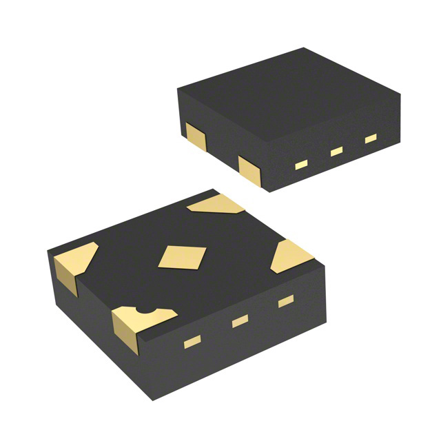
- Package: SOT-23-5
- Essence: High-Speed CMOS Logic
- Packaging/Quantity: Tape and Reel, 3000 pieces per reel
Specifications
- Supply Voltage Range: 1.65V to 5.5V
- Input Voltage Range: 0V to VCC
- Output Voltage Range: 0V to VCC
- Maximum Operating Frequency: 400 MHz
- Propagation Delay: 3.8 ns (typical)
- Output Drive Capability: ±24 mA
- Operating Temperature Range: -40°C to +85°C
Detailed Pin Configuration
The SN74LVC1G125DPWR has a total of 5 pins:
- GND: Ground pin
- OE: Output Enable pin
- A: Input pin
- Y: Output pin
- VCC: Power supply pin
Functional Features
- Non-inverting buffer with tri-state output
- Allows bidirectional data flow
- Supports voltage level translation
- Provides high-speed operation
- Low power consumption
- Schmitt-trigger input for noise immunity
Advantages
- Small package size allows for space-saving designs
- Wide operating voltage range enables compatibility with various systems
- High-speed operation facilitates fast data transmission
- Tri-state output allows multiple devices to share a common bus
- Low power consumption helps prolong battery life in portable applications
Disadvantages
- Limited output drive capability may not be suitable for driving heavy loads
- Single gate configuration restricts the number of inputs/outputs available
Working Principles
The SN74LVC1G125DPWR is a single gate buffer with a non-inverting tri-state output. It operates on the principle of CMOS logic, which uses complementary pairs of MOSFETs to achieve high-speed and low-power operation. The input signal is amplified and inverted by the internal circuitry, and the output can be enabled or disabled using the OE pin. When the OE pin is high, the output is in the high-impedance state, allowing other devices to drive the bus. When the OE pin is low, the output follows the input signal.
Detailed Application Field Plans
The SN74LVC1G125DPWR is commonly used in various applications, including:
- Communication systems: It can be used as a level shifter to interface between different voltage domains in communication circuits.
- Microcontrollers: It can act as a buffer to amplify and invert signals from microcontroller pins.
- Data acquisition systems: It can be employed to isolate and condition analog signals before digitization.
- Industrial automation: It can serve as a driver for controlling actuators and sensors in industrial control systems.
- Automotive electronics: It can be utilized in automotive modules for signal buffering and level translation.
Detailed and Complete Alternative Models
- SN74LVC1G07DBVR: Single Buffer/Driver with Open-Drain Output
- SN74LVC1G04DCKR: Single Inverter Gate
- SN74LVC1G17DBVR: Single Schmitt-Trigger Buffer/Driver
- SN74LVC1G08DCKR: Single 2-Input AND Gate
- SN74LVC1G86DBVR: Single 2-Input Exclusive-OR Gate
These alternative models offer similar functionality and can be considered as substitutes for the SN74LVC1G125DPWR depending on specific requirements.
Word count: 440
Перечислите 10 распространенных вопросов и ответов, связанных с применением SN74LVC1G125DPWR в технических решениях.
Sure! Here are 10 common questions and answers related to the application of SN74LVC1G125DPWR:
Q1: What is SN74LVC1G125DPWR? A1: SN74LVC1G125DPWR is a single bus buffer gate with 3-state output. It is commonly used in digital logic circuits for signal buffering and level shifting.
Q2: What is the operating voltage range of SN74LVC1G125DPWR? A2: The operating voltage range of SN74LVC1G125DPWR is from 1.65V to 5.5V.
Q3: What is the maximum output current of SN74LVC1G125DPWR? A3: The maximum output current of SN74LVC1G125DPWR is 32mA.
Q4: Can SN74LVC1G125DPWR be used as a level shifter? A4: Yes, SN74LVC1G125DPWR can be used as a level shifter to convert signals between different voltage levels.
Q5: What is the propagation delay of SN74LVC1G125DPWR? A5: The propagation delay of SN74LVC1G125DPWR is typically around 4.3ns.
Q6: Is SN74LVC1G125DPWR compatible with both CMOS and TTL logic levels? A6: Yes, SN74LVC1G125DPWR is compatible with both CMOS (0V to Vcc) and TTL (0V to 5V) logic levels.
Q7: Can SN74LVC1G125DPWR drive capacitive loads? A7: Yes, SN74LVC1G125DPWR can drive capacitive loads up to 50pF.
Q8: Does SN74LVC1G125DPWR have built-in ESD protection? A8: Yes, SN74LVC1G125DPWR has built-in ESD protection to prevent damage from electrostatic discharge.
Q9: Can SN74LVC1G125DPWR be used in battery-powered applications? A9: Yes, SN74LVC1G125DPWR is suitable for battery-powered applications due to its low power consumption.
Q10: What is the package type of SN74LVC1G125DPWR? A10: SN74LVC1G125DPWR is available in a small SOT-23-5 package.