

Подробную информацию о продукте см. в характеристиках.
SN74LVC1G373YZTR
Product Overview
- Category: Integrated Circuit
- Use: Logic Level Shifter
- Characteristics: Low Voltage, High-Speed, Single-Gate, Transparent Latch
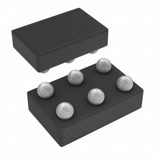
- Package: 8-pin DSBGA (MicroStar Junior™)
- Essence: The SN74LVC1G373YZTR is a single-gate transparent latch that operates at low voltage levels and provides high-speed logic level shifting capabilities.
- Packaging/Quantity: Tape and Reel, 3000 units per reel
Specifications
- Supply Voltage Range: 1.65V to 5.5V
- High-Level Input Voltage: 0.7 x Vcc
- Low-Level Input Voltage: 0.3 x Vcc
- Output Drive Capability: ±24mA
- Operating Temperature Range: -40°C to +125°C
Detailed Pin Configuration
The SN74LVC1G373YZTR has the following pin configuration:
____
   OE |1  8| VCC
  A1  |2  7| Q
  LE  |3  6| D
 GND  |4  5| NC
       ----
Functional Features
- Single-gate transparent latch with an output enable (OE) input
- Allows data to be latched when the latch enable (LE) input is high
- Provides level shifting between different voltage domains
- Supports bidirectional data flow
- High-speed operation for efficient data transfer
Advantages and Disadvantages
Advantages: - Low voltage operation allows compatibility with various systems - High-speed performance enables quick data transfer - Small package size saves board space - Bidirectional data flow simplifies circuit design
Disadvantages: - Limited output drive capability may restrict use in certain applications - Single-gate design may not be suitable for complex logic operations
Working Principles
The SN74LVC1G373YZTR is a transparent latch that operates by latching data when the latch enable (LE) input is high. The output enable (OE) input controls the output state, allowing bidirectional data flow between different voltage domains. The device operates at low voltage levels, making it compatible with a wide range of systems. Its high-speed operation ensures efficient data transfer.
Detailed Application Field Plans
The SN74LVC1G373YZTR can be used in various applications, including but not limited to: - Level shifting in mixed-voltage systems - Data buffering and storage in microcontrollers and digital signal processors - Interface conversion between different logic families - Signal isolation in communication systems - Clock gating and synchronization circuits
Detailed and Complete Alternative Models
Some alternative models that offer similar functionality to the SN74LVC1G373YZTR include: - SN74LVC1G373DBVR - SN74LVC1G373DCKR - SN74LVC1G373DRLR - SN74LVC1G373DCKRG4 - SN74LVC1G373DRLRG4
These alternatives provide comparable features and can be considered based on specific application requirements.
Word count: 335 words
Перечислите 10 распространенных вопросов и ответов, связанных с применением SN74LVC1G373YZTR в технических решениях.
Sure! Here are 10 common questions and answers related to the application of SN74LVC1G373YZTR in technical solutions:
Q1: What is SN74LVC1G373YZTR? A1: SN74LVC1G373YZTR is a single D-type latch with 3-state output, designed for use in various digital applications.
Q2: What is the operating voltage range of SN74LVC1G373YZTR? A2: The operating voltage range of SN74LVC1G373YZTR is from 1.65V to 5.5V.
Q3: What is the maximum output current of SN74LVC1G373YZTR? A3: The maximum output current of SN74LVC1G373YZTR is 32mA.
Q4: Can SN74LVC1G373YZTR be used as a level shifter? A4: Yes, SN74LVC1G373YZTR can be used as a level shifter to convert signals between different voltage levels.
Q5: How many inputs does SN74LVC1G373YZTR have? A5: SN74LVC1G373YZTR has one data input (D) and one enable input (E).
Q6: What is the purpose of the 3-state output feature in SN74LVC1G373YZTR? A6: The 3-state output feature allows the output to be disconnected from the rest of the circuit, enabling multiple devices to share a common bus.
Q7: What is the typical propagation delay of SN74LVC1G373YZTR? A7: The typical propagation delay of SN74LVC1G373YZTR is around 4.8ns.
Q8: Can SN74LVC1G373YZTR be used in high-speed applications? A8: Yes, SN74LVC1G373YZTR is designed for high-speed operation and can be used in various high-frequency applications.
Q9: Is SN74LVC1G373YZTR compatible with other logic families? A9: Yes, SN74LVC1G373YZTR is compatible with both TTL and CMOS logic families.
Q10: What is the package type of SN74LVC1G373YZTR? A10: SN74LVC1G373YZTR is available in a small SOT-23 package, which is suitable for space-constrained applications.
Please note that these answers are general and may vary depending on specific application requirements.