

Подробную информацию о продукте см. в характеристиках.
SN74LVC1G374YEPR
Product Overview
- Category: Integrated Circuit (IC)
- Use: Flip-Flop
- Characteristics: Single-Gate, Low-Voltage, CMOS Logic
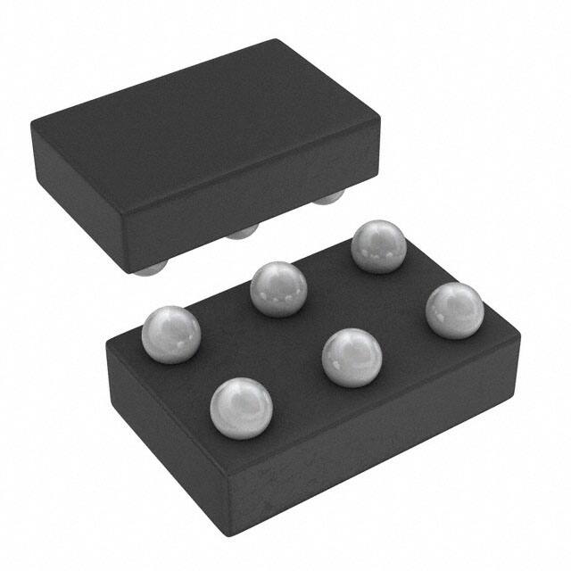
- Package: 8-pin, D-Type Flip-Flop
- Essence: High-performance, low-power consumption flip-flop
- Packaging/Quantity: Tape and Reel, 2500 units per reel
Specifications
- Supply Voltage Range: 1.65V to 5.5V
- Input Voltage Range: 0V to VCC
- Output Voltage Range: 0V to VCC
- Operating Temperature Range: -40°C to +85°C
- Propagation Delay Time: 4.3ns (typical)
- Output Drive Capability: ±24mA at 3.3V
- Power Dissipation: 2.5mW (typical)
Detailed Pin Configuration
The SN74LVC1G374YEPR has the following pin configuration:
```
| | --| CLR Q |-- --| D GND |-- --| CP VCC |-- --| OE /Q |-- --| D |-- --| Q |-- --| GND|-- |___________| ```
Functional Features
- Single positive-edge-triggered D-type flip-flop
- Clear (CLR) input for synchronous reset
- Clock (CP) input for triggering the flip-flop
- Data (D) input for storing the data
- Output Enable (OE) input for enabling/disabling the outputs
- Complementary outputs (Q and /Q) for storing the data
Advantages and Disadvantages
Advantages: - High-performance operation - Low-voltage operation - Low-power consumption - Small package size - Wide operating temperature range
Disadvantages: - Limited output drive capability - Single flip-flop functionality
Working Principles
The SN74LVC1G374YEPR is a single-gate D-type flip-flop that operates on a positive-edge-triggered clock signal. When the clock input (CP) transitions from low to high, the data input (D) is stored in the flip-flop and reflected at the outputs (Q and /Q). The clear input (CLR) can be used to reset the flip-flop synchronously. The output enable input (OE) allows for enabling or disabling the outputs.
Detailed Application Field Plans
The SN74LVC1G374YEPR is commonly used in various digital systems where a single flip-flop is required. Some of its application fields include:
- Microcontrollers: Used for storing and manipulating data in microcontroller circuits.
- Communication Systems: Employed in data transmission and reception circuits.
- Memory Modules: Integrated into memory modules for data storage and retrieval.
- Industrial Automation: Utilized in control systems for sequential logic operations.
- Consumer Electronics: Found in devices like smartphones, tablets, and gaming consoles.
Detailed and Complete Alternative Models
- SN74LVC1G175DBVR: Similar single-gate D-type flip-flop with different package and pin configuration.
- SN74LVC1G273DCKR: Octal D-type flip-flop with similar characteristics but multiple flip-flops in one package.
- SN74LVC1G80DBVR: Single-gate JK flip-flop with similar voltage range and package.
These alternative models provide similar functionality and can be considered as substitutes for the SN74LVC1G374YEPR in different applications.
Word count: 446 words
Перечислите 10 распространенных вопросов и ответов, связанных с применением SN74LVC1G374YEPR в технических решениях.
Sure! Here are 10 common questions and answers related to the application of SN74LVC1G374YEPR in technical solutions:
Q1: What is SN74LVC1G374YEPR? A1: SN74LVC1G374YEPR is a single D-type flip-flop with 3-state output, designed for low-voltage (1.65V to 5.5V) applications.
Q2: What is the purpose of SN74LVC1G374YEPR? A2: SN74LVC1G374YEPR is used to store and control digital data in various electronic circuits and systems.
Q3: What are the key features of SN74LVC1G374YEPR? A3: Some key features include high-speed operation, low power consumption, wide operating voltage range, and 3-state outputs.
Q4: What is the maximum operating frequency of SN74LVC1G374YEPR? A4: The maximum operating frequency of SN74LVC1G374YEPR is typically around 400 MHz.
Q5: How many flip-flops are there in SN74LVC1G374YEPR? A5: SN74LVC1G374YEPR consists of a single D-type flip-flop.
Q6: Can SN74LVC1G374YEPR be used in both input and output applications? A6: Yes, SN74LVC1G374YEPR can be used as both an input and output device depending on the circuit configuration.
Q7: What is the output drive capability of SN74LVC1G374YEPR? A7: SN74LVC1G374YEPR has a typical output drive capability of ±24 mA.
Q8: Is SN74LVC1G374YEPR compatible with other logic families? A8: Yes, SN74LVC1G374YEPR is compatible with a wide range of logic families due to its 3.3V and 5V tolerant inputs.
Q9: Can SN74LVC1G374YEPR be used in battery-powered applications? A9: Yes, SN74LVC1G374YEPR is suitable for battery-powered applications due to its low power consumption characteristics.
Q10: What are some typical applications of SN74LVC1G374YEPR? A10: Some typical applications include data storage, address latching, signal buffering, level shifting, and general-purpose digital logic circuits.
Please note that the answers provided here are general and may vary depending on specific circuit requirements and design considerations.