

Подробную информацию о продукте см. в характеристиках.
SN74LVC1G74DQER
Product Overview
Category
The SN74LVC1G74DQER belongs to the category of integrated circuits (ICs), specifically digital logic gates.
Use
This product is commonly used in electronic devices and systems for signal processing, data manipulation, and control functions. It serves as a flip-flop, which is a fundamental building block in digital circuits.
Characteristics
- Low-voltage CMOS technology: The SN74LVC1G74DQER operates at low voltage levels, making it suitable for battery-powered applications.
- High-speed operation: This IC offers fast switching times, enabling efficient data processing.
- Small form factor: The compact package size allows for space-saving integration into various electronic designs.
- Wide operating temperature range: The SN74LVC1G74DQER can operate reliably across a broad temperature spectrum.
Package and Quantity
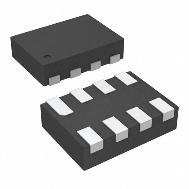
The SN74LVC1G74DQER is available in a small outline package (SOT) with 6 pins. It is typically sold in reels or tubes, with quantities varying depending on the supplier.
Specifications
- Supply Voltage Range: 1.65V to 5.5V
- Input Voltage Range: 0V to VCC
- Output Voltage Range: 0V to VCC
- Operating Temperature Range: -40°C to +85°C
- Maximum Propagation Delay: 4.3 ns (typical)
- Maximum Power Dissipation: 500mW
Detailed Pin Configuration
The SN74LVC1G74DQER has six pins, labeled as follows:
- GND: Ground connection
- D: Data input
- CP: Clock pulse input
- Q: Output
- PRE: Preset input
- CLR: Clear input
Functional Features
The SN74LVC1G74DQER is a positive-edge-triggered D-type flip-flop. It stores and outputs data based on the clock pulse input (CP). The data input (D) determines the state of the flip-flop, which is then latched and reflected at the output (Q). The preset (PRE) and clear (CLR) inputs allow for additional control over the flip-flop's behavior.
Advantages and Disadvantages
Advantages
- Low power consumption: The SN74LVC1G74DQER operates efficiently, making it suitable for battery-powered devices.
- Compact size: Its small form factor enables integration into space-constrained designs.
- High-speed operation: The IC offers fast switching times, facilitating rapid data processing.
Disadvantages
- Single-bit functionality: The SN74LVC1G74DQER is designed to handle only one bit of data at a time, limiting its application in complex systems requiring multiple bits of storage.
Working Principles
The SN74LVC1G74DQER operates based on the principles of sequential logic. When the clock pulse input (CP) transitions from low to high (positive edge), the data input (D) is sampled and stored in the flip-flop. The stored value is then available at the output (Q) until the next clock pulse triggers a new data update.
Detailed Application Field Plans
The SN74LVC1G74DQER finds applications in various electronic systems, including but not limited to: - Microcontrollers and microprocessors - Communication devices - Consumer electronics - Industrial automation - Automotive electronics
In microcontrollers and microprocessors, this flip-flop can be used for register storage, synchronization, and control purposes. In communication devices, it aids in signal processing and data manipulation. Consumer electronics, such as smartphones and tablets, can utilize the SN74LVC1G74DQER for efficient data handling. In industrial automation, it contributes to control systems and timing circuits. Automotive electronics benefit from this IC in areas like engine management and driver assistance systems.
Detailed and Complete Alternative Models
- SN74LVC1G74DBVR
- SN74LVC1G74DCKR
- SN74LVC1G74DRLR
- SN74LVC1G74DRYR
- SN74LVC1G74DRLRG4
- SN74LVC1G74DCKRG4
These alternative models offer similar functionality and characteristics to the SN74LVC1G74DQER, providing options for different package types or supplier preferences.
In conclusion, the SN74LVC1G74DQER is a versatile digital logic gate that serves as a flip-flop in various electronic applications. Its low-voltage operation, high-speed performance, and compact size make it an attractive choice for designers seeking efficient and space-saving solutions.
Перечислите 10 распространенных вопросов и ответов, связанных с применением SN74LVC1G74DQER в технических решениях.
Sure! Here are 10 common questions and answers related to the application of SN74LVC1G74DQER in technical solutions:
1. What is SN74LVC1G74DQER? - SN74LVC1G74DQER is a single positive-edge-triggered D-type flip-flop with clear and preset, designed for 1.65-V to 5.5-V VCC operation.
2. What are the key features of SN74LVC1G74DQER? - The key features include low power consumption, wide operating voltage range, high-speed operation, and compatibility with various logic families.
3. What is the maximum operating frequency of SN74LVC1G74DQER? - The maximum operating frequency of SN74LVC1G74DQER is typically 400 MHz.
4. How many flip-flops are there in SN74LVC1G74DQER? - SN74LVC1G74DQER consists of a single flip-flop.
5. What is the purpose of the clear and preset inputs in SN74LVC1G74DQER? - The clear input allows you to asynchronously reset the flip-flop, while the preset input allows you to set the flip-flop to a specific state.
6. Can SN74LVC1G74DQER be used in battery-powered applications? - Yes, SN74LVC1G74DQER is suitable for battery-powered applications as it operates at low power and has a wide operating voltage range.
7. Is SN74LVC1G74DQER compatible with other logic families? - Yes, SN74LVC1G74DQER is compatible with various logic families such as TTL, CMOS, and LVCMOS.
8. What is the typical propagation delay of SN74LVC1G74DQER? - The typical propagation delay of SN74LVC1G74DQER is around 3.5 ns.
9. Can SN74LVC1G74DQER be used in high-speed applications? - Yes, SN74LVC1G74DQER is designed for high-speed operation and can be used in applications that require fast switching.
10. Are there any recommended operating conditions for SN74LVC1G74DQER? - Yes, some recommended operating conditions include a supply voltage range of 1.65 V to 5.5 V, an input voltage range of 0 V to VCC, and an operating temperature range of -40°C to 125°C.
Please note that these answers are general and may vary depending on specific application requirements.