

Подробную информацию о продукте см. в характеристиках.
SN74LVC2G74YZAR
Product Overview
- Category: Integrated Circuit (IC)
- Use: Flip-Flop
- Characteristics: Low-voltage, dual positive-edge-triggered D-type flip-flop
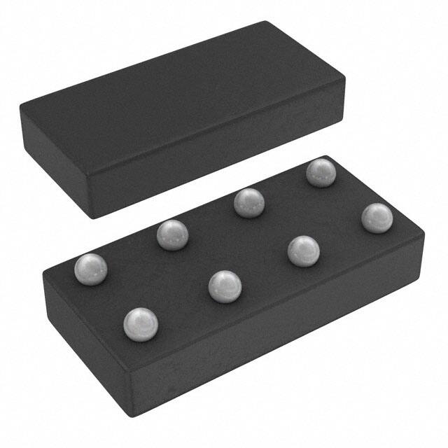
- Package: 8-pin small-outline integrated circuit (SOIC)
- Essence: This IC is designed to store and transfer data in electronic circuits.
- Packaging/Quantity: Available in tape and reel packaging with a quantity of 2500 units per reel.
Specifications
- Supply Voltage Range: 1.65V to 5.5V
- High-Level Input Voltage: 0.7 x Vcc
- Low-Level Input Voltage: 0.3 x Vcc
- High-Level Output Voltage: 0.9 x Vcc
- Low-Level Output Voltage: 0.1 x Vcc
- Maximum Operating Frequency: 100 MHz
- Propagation Delay Time: 4.6 ns
- Operating Temperature Range: -40°C to +85°C
Detailed Pin Configuration
The SN74LVC2G74YZAR has the following pin configuration:
___________
      |           |
   1 -| CLR       |-
   2 -| D         |-
   3 -| CP        |-
   4 -| Q         |-
   5 -| Q̅        |-
   6 -| GND       |-
   7 -| VCC       |-
      |___________|
Functional Features
- Dual positive-edge-triggered D-type flip-flop with clear (CLR) input
- Data (D) input for each flip-flop
- Clock (CP) input for controlling the flip-flop operation
- Outputs (Q and Q̅) provide the stored data
- Clear (CLR) input resets the flip-flop to a known state
Advantages and Disadvantages
Advantages: - Low-voltage operation allows for compatibility with various electronic systems - Small package size enables space-saving designs - High operating frequency allows for fast data transfer - Clear input provides a convenient way to reset the flip-flop
Disadvantages: - Limited number of flip-flops in a single IC package - Not suitable for high-power applications due to low voltage operation
Working Principles
The SN74LVC2G74YZAR operates based on positive-edge-triggered D-type flip-flop logic. The flip-flop stores and transfers data based on the clock signal (CP) and data input (D). When the clock signal transitions from low to high, the data at the D input is captured and stored in the flip-flop. The stored data is then available at the outputs (Q and Q̅). The clear input (CLR) can be used to reset the flip-flop to a known state.
Detailed Application Field Plans
The SN74LVC2G74YZAR is commonly used in various digital systems and applications, including but not limited to: - Microcontrollers - Data storage devices - Communication systems - Consumer electronics - Industrial automation
Detailed and Complete Alternative Models
Some alternative models that serve similar functions to the SN74LVC2G74YZAR include: - MC74VHC1G74: Single positive-edge-triggered D-type flip-flop - CD4013B: Dual D-type flip-flop with set and reset inputs - 74HC74: Dual D-type flip-flop with clear input
These alternative models offer different specifications and features, allowing designers to choose the most suitable option for their specific application requirements.
Word count: 389 words
Перечислите 10 распространенных вопросов и ответов, связанных с применением SN74LVC2G74YZAR в технических решениях.
Sure! Here are 10 common questions and answers related to the application of SN74LVC2G74YZAR in technical solutions:
Q: What is SN74LVC2G74YZAR? A: SN74LVC2G74YZAR is a dual positive-edge-triggered D-type flip-flop integrated circuit (IC) manufactured by Texas Instruments.
Q: What is the operating voltage range for SN74LVC2G74YZAR? A: The operating voltage range for SN74LVC2G74YZAR is typically between 1.65V and 5.5V.
Q: What is the maximum clock frequency supported by SN74LVC2G74YZAR? A: SN74LVC2G74YZAR can support clock frequencies up to 100 MHz.
Q: Can SN74LVC2G74YZAR be used as a level shifter? A: Yes, SN74LVC2G74YZAR can be used as a level shifter to convert signals between different voltage levels.
Q: How many flip-flops are present in SN74LVC2G74YZAR? A: SN74LVC2G74YZAR contains two independent D-type flip-flops.
Q: What is the typical propagation delay of SN74LVC2G74YZAR? A: The typical propagation delay of SN74LVC2G74YZAR is around 4.7 ns.
Q: Is SN74LVC2G74YZAR suitable for high-speed applications? A: Yes, SN74LVC2G74YZAR is designed for high-speed operation and can be used in various high-frequency applications.
Q: Can SN74LVC2G74YZAR be used in battery-powered devices? A: Yes, SN74LVC2G74YZAR has a low power consumption and can be used in battery-powered devices.
Q: What is the package type of SN74LVC2G74YZAR? A: SN74LVC2G74YZAR is available in a small-outline transistor (SOT) package.
Q: Are there any recommended applications for SN74LVC2G74YZAR? A: SN74LVC2G74YZAR is commonly used in applications such as data storage, clock synchronization, and general-purpose digital logic circuits.
Please note that these answers are general and may vary depending on specific design requirements and application scenarios.